DLPS159D April 2019 – December 2024 DLP470NE
PRODUCTION DATA
- 1
- 1 Features
- 2 Applications
- 3 Description
- 4 Pin Configuration and Functions
-
5 Specifications
- 5.1 Absolute Maximum Ratings
- 5.2 Storage Conditions
- 5.3 ESD Ratings
- 5.4 Recommended Operating Conditions
- 5.5 Thermal Information
- 5.6 Electrical Characteristics
- 5.7 Capacitance at Recommended Operating Conditions
- 5.8 Timing Requirements
- 5.9 System Mounting Interface Loads
- 5.10 Micromirror Array Physical Characteristics
- 5.11 Micromirror Array Optical Characteristics
- 5.12 Window Characteristics
- 5.13 Chipset Component Usage Specification
- 6 Detailed Description
- 7 Application and Implementation
- 8 Power Supply Recommendations
- 9 Layout
- 10Device and Documentation Support
- 11Revision History
- Mechanical, Packaging, and Orderable Information
Package Options
Mechanical Data (Package|Pins)
- FXH|257
Thermal pad, mechanical data (Package|Pins)
Orderable Information
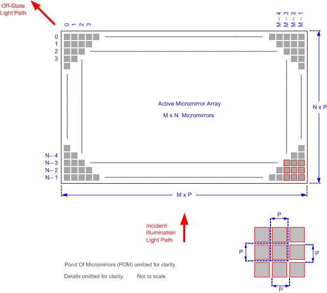
5.10 Micromirror Array Physical Characteristics
Table 5-2 Micromirror Array Physical Characteristics
| PARAMETER DESCRIPTION | VALUE | UNIT | |
|---|---|---|---|
| Number of active columns (1) | M | 1920 | micromirrors |
| Number of active rows (1) | N | 1080 | micromirrors |
| Micromirror (pixel) pitch (1) | P | 5.4 | µm |
| Micromirror active array width (1) | Micromirror Pitch × number of active columns | 10.368 | mm |
| Micromirror active array height (1) | Micromirror Pitch × number of active rows | 5.832 | mm |
| Micromirror active border (Top / Bottom) (2) | Pond of micromirrors (POM) | 80 | micromirrors/side |
| Micromirror active border (Right / Left) (2) | Pond of micromirrors (POM) | 84 | micromirrors/side |
(1) See Figure 5-8.
(2) The structure and qualities of the border around the active array includes a
band of partially functional micromirrors referred to as the Pond Of
Mirrors (POM). These micromirrors are structurally and electrically
prevented from tilting toward the bright or ON state but still require an
electrical bias to tilt toward the OFF state.
 Figure 5-8 Micromirror Array Physical Characteristics