DLPS247 August 2024 DLP472TP
PRODUCTION DATA
- 1
- 1 Features
- 2 Applications
- 3 Description
- 4 Pin Configuration and Functions
-
5 Specifications
- 5.1 Absolute Maximum Ratings
- 5.2 Storage Conditions
- 5.3 ESD Ratings
- 5.4 Recommended Operating Conditions
- 12
- 5.5 Thermal Information
- 5.6 Electrical Characteristics
- 5.7 Switching Characteristics
- 5.8 Timing Requirements
- 17
- 5.9 System Mounting Interface Loads
- 19
- 5.10 Micromirror Array Physical Characteristics
- 21
- 5.11 Micromirror Array Optical Characteristics
- 23
- 5.12 Window Characteristics
- 5.13 Chipset Component Usage Specification
- 6 Detailed Description
- 7 Application and Implementation
- 8 Power Supply Recommendations
- 9 Layout
- 10Device and Documentation Support
- 11Revision History
- 12Mechanical, Packaging, and Orderable Information
Package Options
Mechanical Data (Package|Pins)
- FQY|174
Thermal pad, mechanical data (Package|Pins)
Orderable Information
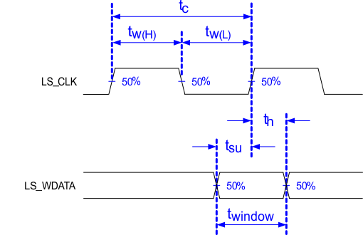
The low-speed interface is LPSDR
and adheres to the Electrical Characteristics and AC/DC Operating Conditions
table in JEDEC Standard No. 209B, Low Power Double Data Rate (LPDDR)
JESD209B.
Figure 5-2 LPSDR Switching Parameters Figure 5-3 LPSDR Input Rise and Fall Slew Rate
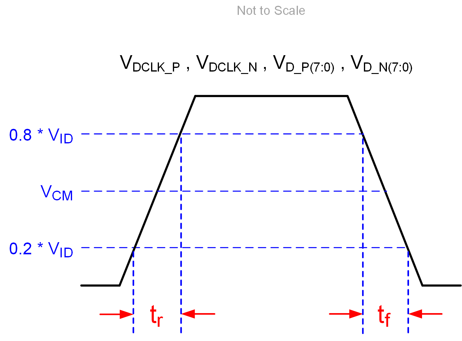 Figure 5-4 SubLVDS Input Rise and Fall Slew Rate
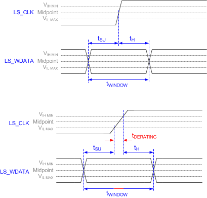 Figure 5-5 Window Time Derating Concept
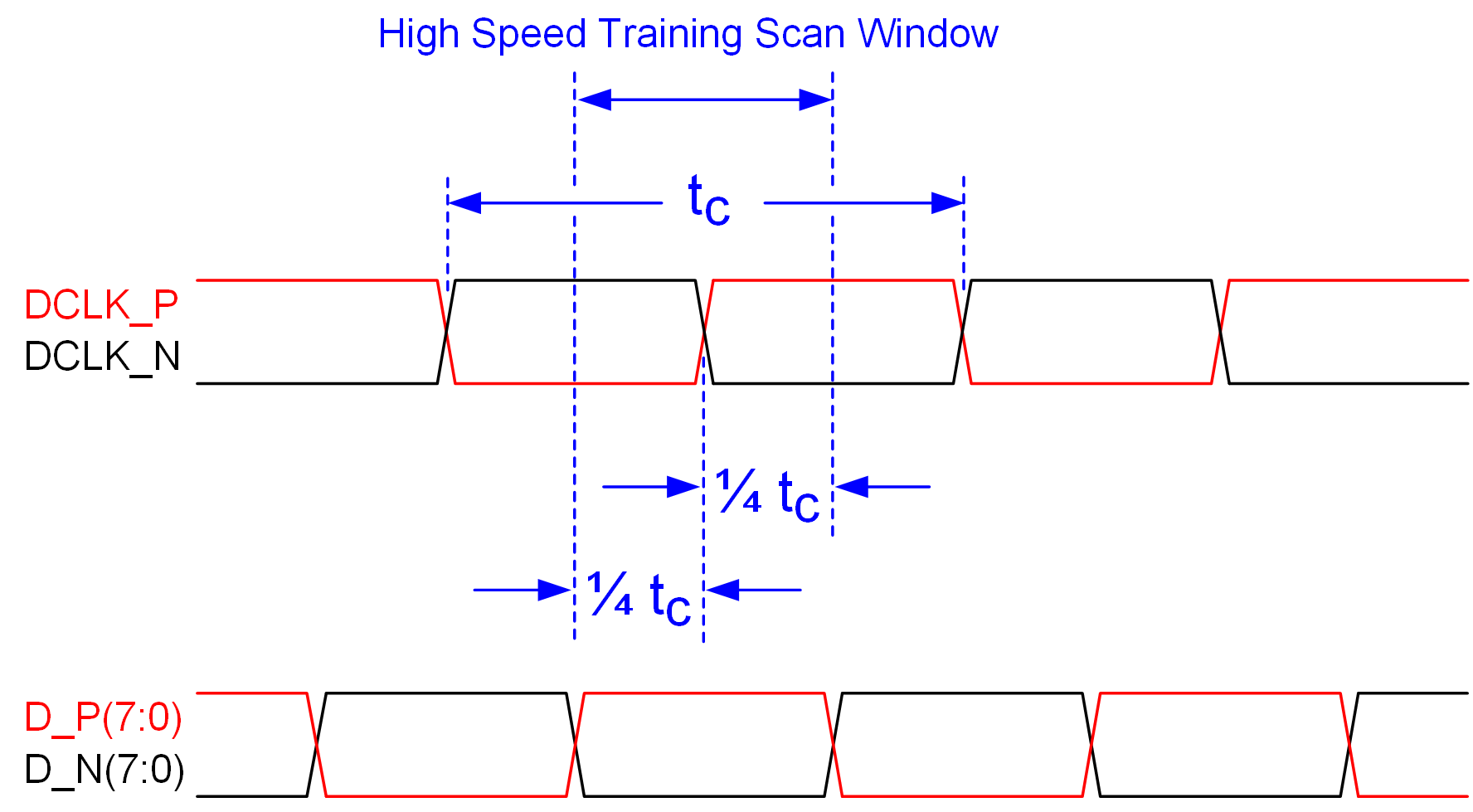
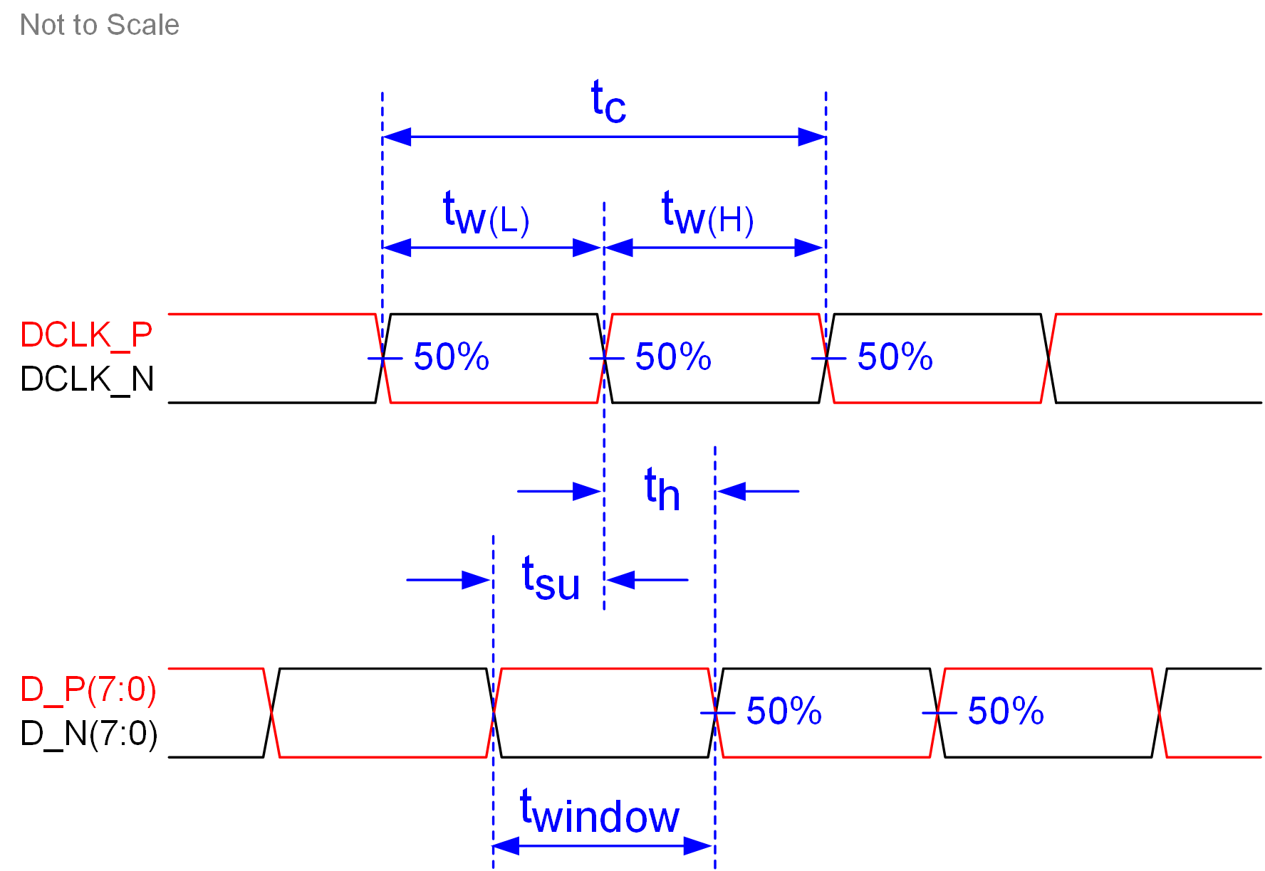 Figure 5-6 SubLVDS Switching Parameters
 Figure 5-8 SubLVDS Voltage Parameters
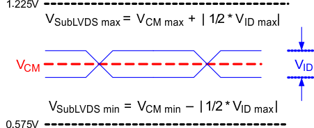 Figure 5-9 SubLVDS Waveform Parameters
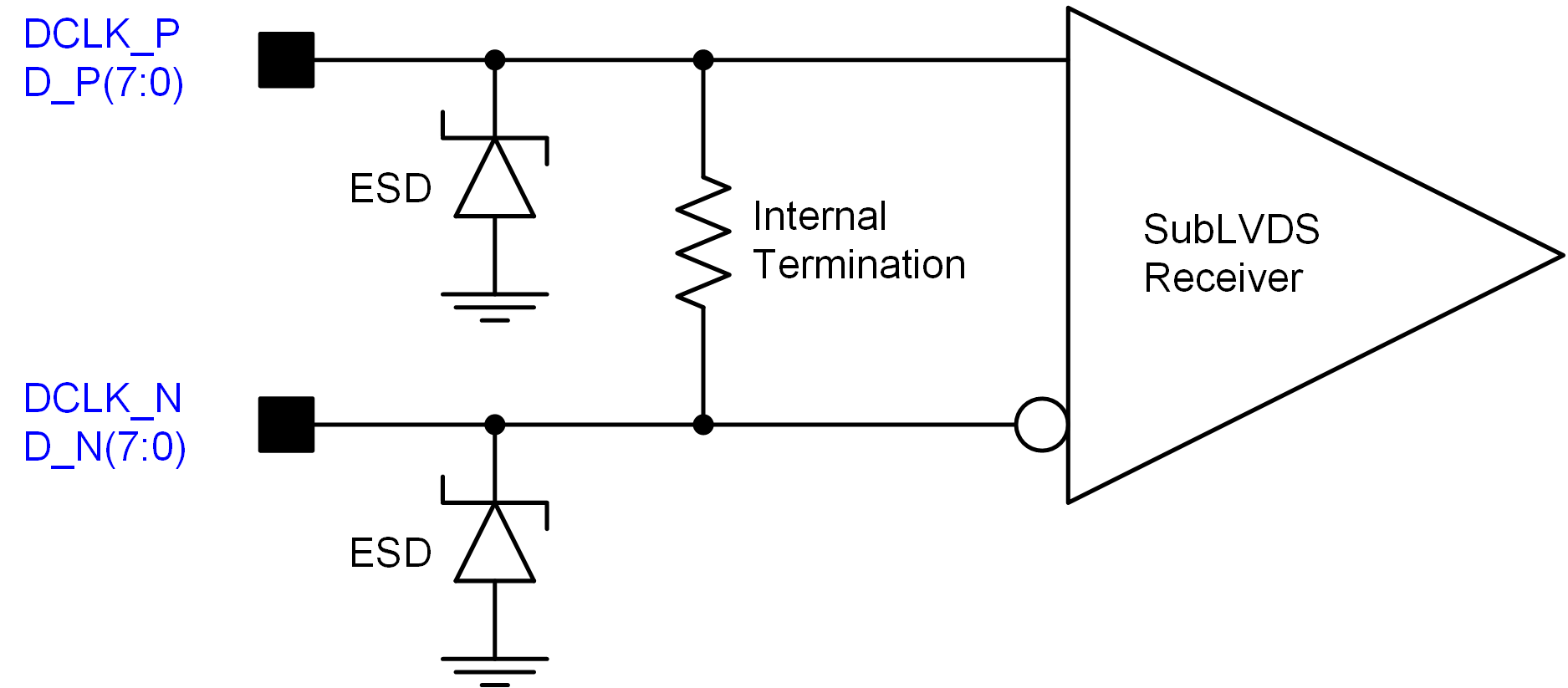 Figure 5-10 SubLVDS Equivalent Input Circuit
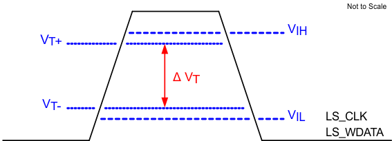 Figure 5-11 LPSDR Input Hysteresis
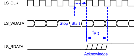 Figure 5-12 LPSDR Read Out
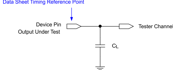
See Section 5.6 for more information.
Figure 5-13 Test Load Circuit for Output Propagation Measurement