DLPS013H April 2010 – December 2024 DLP5500
PRODUCTION DATA
- 1
- 1 Features
- 2 Applications
- 3 Description
- 4 Description (continued)
- 5 Pin Configuration and Functions
-
6 Specifications
- 6.1 Absolute Maximum Ratings
- 6.2 Storage Conditions
- 6.3 ESD Ratings
- 6.4 Recommended Operating Conditions
- 6.5 Thermal Information
- 6.6 Electrical Characteristics
- 6.7 Timing Requirements
- 6.8 System Mounting Interface Loads
- 6.9 Micromirror Array Physical Characteristics
- 6.10 Micromirror Array Optical Characteristics
- 6.11 Window Characteristics
- 6.12 Chipset Component Usage Specification
- 7 Detailed Description
- 8 Application and Implementation
- 9 Power Supply Recommendations
- 10Layout
- 11Device and Documentation Support
- 12Revision History
- 13Mechanical, Packaging, and Orderable Information
Package Options
Mechanical Data (Package|Pins)
- FYA|149
Thermal pad, mechanical data (Package|Pins)
Orderable Information
6.6 Electrical Characteristics
over operating free-air temperature range (unless otherwise noted)
| PARAMETER | TEST CONDITIONS | MIN | TYP | MAX | UNIT | ||
|---|---|---|---|---|---|---|---|
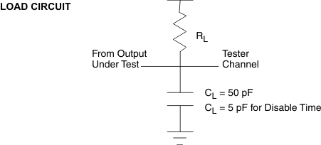
| VOH | High-level output voltage(1), See Figure 6-2 | VCC = 3.0 V, | IOH = –20 mA | 2.4 | V | ||
| VOL | Low-level output voltage(1), See Figure 6-2 | VCC = 3.6 V, | IOL = 15 mA | 0.4 | V | ||
| IOZ | High impedance output current(1) | VCC = 3.6 V | 10 | µA | |||
| IIL | Low-level input current(1) | VCC = 3.6 V, | VI = 0 V | –60 | µA | ||
| IIH | High-level input current(1) | VCC = 3.6 V, | VI = VCC | 200 | µA | ||
| ICC | Current into VCC pin | VCC = 3.6 V, | 750 | mA | |||
| ICCI | Current into VOFFSET pin(2) | VCCI = 3.6 V | 450 | mA | |||
| ICC2 | Current into VCC2 pin | VCC2 = 8.75V | 25 | mA | |||
| ZIN | Internal Differential Impedance | 95 | 105 | Ω | |||
| ZLINE | Line Differential Impedance (PWB or Trace) | 90 | 100 | 110 | Ω | ||
| CI | Input capacitance(1) | f = 1 MHz | 10 | pF | |||
| CO | Output capacitance(1) | f = 1 MHz | 10 | pF | |||
| CIM | Input capacitance for MBRST[0:15] pins | f = 1 MHz | 160 | 210 | pF | ||
(1) Applies to LVCMOS pins only
(2) Exceeding the maximum allowable absolute voltage difference between VCC and VCCI may result in excess current draw. (Refer to Absolute Maximum Ratings for details)
 Figure 6-2 Measurement Condition for LVCMOS Output