DLPS013H April 2010 – December 2024 DLP5500
PRODUCTION DATA
- 1
- 1 Features
- 2 Applications
- 3 Description
- 4 Description (continued)
- 5 Pin Configuration and Functions
-
6 Specifications
- 6.1 Absolute Maximum Ratings
- 6.2 Storage Conditions
- 6.3 ESD Ratings
- 6.4 Recommended Operating Conditions
- 6.5 Thermal Information
- 6.6 Electrical Characteristics
- 6.7 Timing Requirements
- 6.8 System Mounting Interface Loads
- 6.9 Micromirror Array Physical Characteristics
- 6.10 Micromirror Array Optical Characteristics
- 6.11 Window Characteristics
- 6.12 Chipset Component Usage Specification
- 7 Detailed Description
- 8 Application and Implementation
- 9 Power Supply Recommendations
- 10Layout
- 11Device and Documentation Support
- 12Revision History
- 13Mechanical, Packaging, and Orderable Information
Package Options
Mechanical Data (Package|Pins)
- FYA|149
Thermal pad, mechanical data (Package|Pins)
Orderable Information
6.10 Micromirror Array Optical Characteristics
TI assumes no responsibility for end-equipment optical performance. Achieving the desired end-equipment optical performance involves making trade-offs between numerous component and system design parameters. See the Application Notes for additional details, considerations, and guidelines: TI DLP® System Design: Optical Module Specifications.
| PARAMETER | CONDITIONS | MIN | NOM | MAX | UNIT |
|---|---|---|---|---|---|
| Micromirror tilt angle, a | DMD parked state(1)(2)(3), see Figure 7-3. | 0 | degrees | ||
| DMD landed state(1)(4)(5), see Figure 7-3. | 12 | ||||
| Micromirror tilt angle variation, b(1)(4)(6)(7)(8) | See Figure 7-3. | –1 | 1 | degrees | |
| Micromirror Cross Over Time(10) | 16 | 22 | µs | ||
| Micromirror Switching Time(11) | 140 | µs | |||
| Non-operating micromirrors(12) | Non-adjacent micromirrors | 10 | micromirrors | ||
| Adjacent micromirrors | 0 | ||||
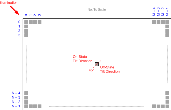
| Orientation of the micromirror axis-of-rotation(9) | See . | 44 | 45 | 46 | degrees |
| Micromirror array optical efficiency(13)(14) | 420 – 700, with all micromirrors in the ON state | 68% | nm | ||
| Mirror metal specular reflectivity | 420 – 700 | 89.4% | nm |
(1) Measured relative to the plane formed by the overall micromirror array
(2) Parking the micromirror array returns all of the micromirrors to an essentially flat (0°) state (as measured relative to the plane formed by the overall micromirror array).
(3) When the micromirror array is parked, the tilt angle of each individual micromirror is uncontrolled.
(4) Additional variation exists between the micromirror array and the package datums,
as shown in the packaging section at the end of the document.
(5) When the micromirror array is landed, the tilt angle of each individual
micromirror is dictated by the binary contents of the CMOS memory cell
associated with each individual micromirror. A binary value of 1 will result in
a micromirror landing in an nominal angular position of +12 degrees. A binary
value of 0 will result in a micromirror landing in an nominal angular position
of –12 degrees.
(6) Represents the landed tilt angle variation relative to the Nominal landed tilt angle.
(7) Represents the variation that can occur between any two individual micromirrors, located on the same device or located on different devices.
(8) For some applications, it is critical to account for the micromirror tilt angle variation in the overall System Optical Design. With some System Optical Designs, the micromirror tilt angle variations within a device may result in perceivable non-uniformities in the light field reflected from the micromirror array. With some System Optical Designs, the micromirror tilt angle variation between devices may result in colorimetry variations and/or system contrast variations.
(9) Measured relative to the package datums B and C, shown in the Section 13 section at the end of this document.
(10) Micromirror Cross Over time is primarily a function of the natural response time of the micromirrors.
(11) Micromirror switching is controlled and coordinated by the DLPC200 (see DLPS014), DLPA200, and DLPS015). Nominal Switching
time depends on the system implementation and represents the time for the entire
micromirror array to be refreshed.
(12) Non-operating micromirror is defined as a micromirror that is unable to
transition nominally from the –12 degree position to +12 degree or vice
versa.
(13) The minimum or maximum DMD optical efficiency observed in a specific application depends on numerous application-specific design variables, such as but not limited to:
- Illumination wavelength, bandwidth or line-width, degree of coherence
- Illumination angle, plus angle tolerance
- Illumination and projection aperture size, and location in the system optical path
- IIlumination overfill of the DMD micromirror array
- Aberrations present in the illumination source and/or path
- Aberrations present in the projection path
- Visible illumination (420nm – 700nm)
- Input illumination optical axis oriented at 24° relative to the window normal
- Projection optical axis oriented at 0° relative to the window normal
- f/3.0 illumination aperture
- f/2.4 projection aperture
- Micromirror array fill factor: nominally 92%
- Micromirror array diffraction efficiency: nominally 86%
- Micromirror surface reflectivity: nominally 88%
- Window transmission: nominally 97% (single pass, through two surface transitions)
(14) Does not account for the effect of micromirror switching duty cycle, which is
application dependent. Micromirror switching duty cycle represents the
percentage of time that the micromirror is actually reflecting light from the
optical illumination path to the optical projection path. This duty cycle
depends on the illumination aperture size, the projection aperture size, and the
micromirror array update rate.

Refer to section Micromirror Array Physical Characteristics table for M, N, and P specifications.
Figure 6-12 Micromirror Landed Orientation and Tilt