DLPS013H April 2010 – December 2024 DLP5500
PRODUCTION DATA
- 1
- 1 Features
- 2 Applications
- 3 Description
- 4 Description (continued)
- 5 Pin Configuration and Functions
-
6 Specifications
- 6.1 Absolute Maximum Ratings
- 6.2 Storage Conditions
- 6.3 ESD Ratings
- 6.4 Recommended Operating Conditions
- 6.5 Thermal Information
- 6.6 Electrical Characteristics
- 6.7 Timing Requirements
- 6.8 System Mounting Interface Loads
- 6.9 Micromirror Array Physical Characteristics
- 6.10 Micromirror Array Optical Characteristics
- 6.11 Window Characteristics
- 6.12 Chipset Component Usage Specification
- 7 Detailed Description
- 8 Application and Implementation
- 9 Power Supply Recommendations
- 10Layout
- 11Device and Documentation Support
- 12Revision History
- 13Mechanical, Packaging, and Orderable Information
Package Options
Mechanical Data (Package|Pins)
- FYA|149
Thermal pad, mechanical data (Package|Pins)
Orderable Information
7.3 Feature Description
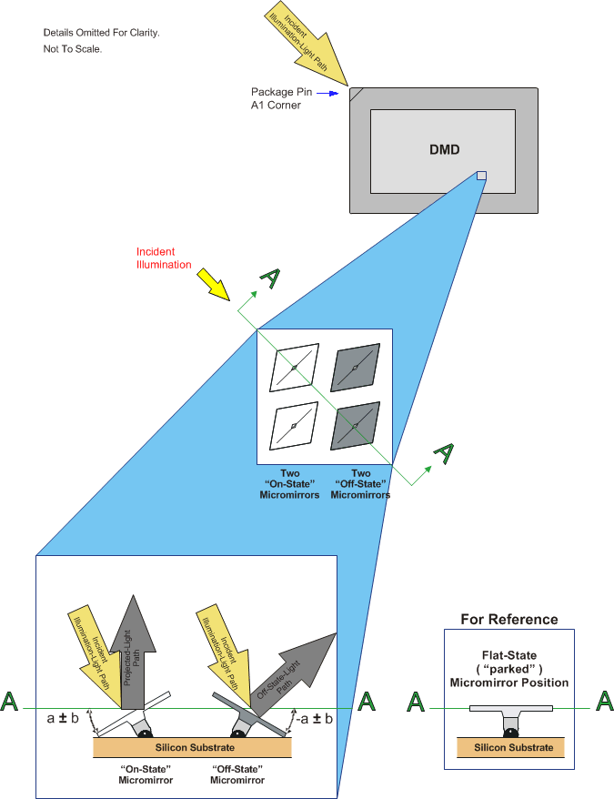
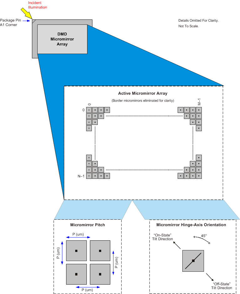
The DLP5500 device consists of 786,432 highly reflective, digitally switchable, micrometer-sized mirrors (micromirrors) organized in a two-dimensional orthogonal pixel array. Refer to Figure 6-11 and Figure 7-2.
Each aluminum micromirror is switchable between two discrete angular positions, –a and +a. The angular positions are measured relative to the micromirror array plane, which is parallel to the silicon substrate. Refer to Micromirror Array Optical Characteristics and Figure 7-3.
The parked position of the micromirror is not a latched position and is therefore not necessarily perfectly parallel to the array plane. Individual micromirror flat state angular positions may vary. Tilt direction of the micromirror is perpendicular to the hinge-axis. The on-state landed position is directed toward the left-top edge of the package, as shown in Figure 7-2.
Each individual micromirror is positioned over a corresponding CMOS memory cell. The angular position of a specific micromirror is determined by the binary state (logic 0 or 1) of the corresponding CMOS memory cell contents, after the mirror clocking pulse is applied. The angular position (–a and +a) of the individual micromirrors changes synchronously with a micromirror clocking pulse, rather than being coincident with the CMOS memory cell data update.
Writing logic 1 into a memory cell followed by a mirror clocking pulse results in the corresponding micromirror switching to the +a position. Writing logic 0 into a memory cell followed by a mirror clocking pulse results in the corresponding micromirror switching to the – a position.
Updating the angular position of the micromirror array consists of two steps. First, update the contents of the CMOS memory. Second, apply a micromirror clocking pulse (reset) to all or a portion of the micromirror array (depending upon the configuration of the system). Micromirror reset pulses are generated externally by the DLPC200 controller in conjunction with the DLPA200 analog driver, with application of the pulses being coordinated by the DLPC200 controller.
For more information, see the TI application report DLPA008, DMD101: Introduction to Digital Micromirror Device (DMD) Technology.

