DLPS036B September 2014 – October 2016 DLP9000
PRODUCTION DATA.
- 1 Features
- 2 Applications
- 3 Description
- 4 Revision History
- 5 Description (continued)
- 6 Pin Configuration and Functions
-
7 Specifications
- 7.1 Absolute Maximum Ratings
- 7.2 Storage Conditions
- 7.3 ESD Ratings
- 7.4 Recommended Operating Conditions
- 7.5 Thermal Information
- 7.6 Electrical Characteristics
- 7.7 Timing Requirements
- 7.8 Capacitance at Recommended Operating Conditions
- 7.9 Typical Characteristics
- 7.10 System Mounting Interface Loads
- 7.11 Micromirror Array Physical Characteristics
- 7.12 Micromirror Array Optical Characteristics
- 7.13 Optical and System Image Quality
- 7.14 Window Characteristics
- 7.15 Chipset Component Usage Specification
- 8 Parameter Measurement Information
- 9 Detailed Description
- 10Application and Implementation
- 11Power Supply Requirements
- 12Layout
- 13Device and Documentation Support
- 14Mechanical, Packaging, and Orderable Information
Package Options
Mechanical Data (Package|Pins)
- FLS|355
Thermal pad, mechanical data (Package|Pins)
Orderable Information
10 Application and Implementation
NOTE
Information in the following applications sections is not part of the TI component specification, and TI does not warrant its accuracy or completeness. TI’s customers are responsible for determining suitability of components for their purposes. Customers should validate and test their design implementation to confirm system functionality.
10.1 Application Information
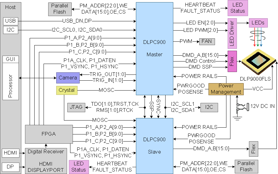
The DLP9000 DMD is controlled by two DLPC900 controllers. This chipset offers two modes of operation. The first is video mode where the video source is displayed on the DMD. The second is Pattern mode, where the patterns are pre-stored in flash memory and then streamed to the DMD. The allowed DMD pattern rate depends on which mode and bit-depth is selected.
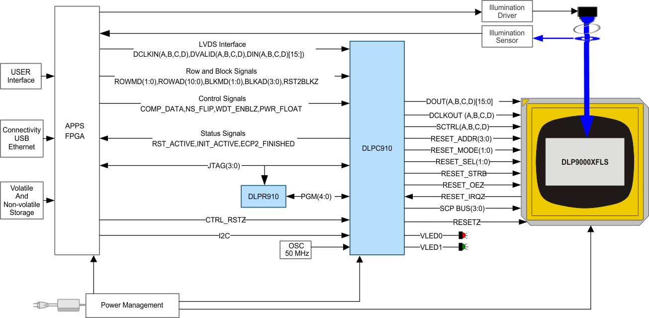
The DLP9000X DMD is controlled by the DLPC910 controller, where the DLPC910 is configured by the program content in the DLPR910. This chipset offers streaming 1-bit binary patterns to the DMD at speeds greater than 61 Gigabits per second (Gbps). The patterns are streamed from an customer designed processor into the DLPC910 LVDS input data interface.
Both the DLP9000 and the DLP9000X provide solutions for many varied applications including structured light,
3-D printing, video projection, and high speed lithography. The DMD is a spatial light modulator, which reflects incoming light from an illumination source to one of two directions, with the primary direction being into a projection or collection optic. Each application is derived primarily from the optical architecture of the system and the format of the data being used.
10.2 Typical Applications
10.2.1 Typical Application using DLP9000
A typical embedded system application using two DLPC900 controllers and a DLP9000 DMD is shown in Figure 17. In this configuration, the DLPC900 controller supports a 24-bit parallel RGB input, typical of LCD interfaces, from an external source or processor. The 24-bit parallel data must be split between a left half and a right half, each half between the two controllers. The external processor must format each half to consist of 1280x1600 plus any horizontal and vertical blanking at half the pixel clock rate. This system configuration supports still and motion video as well as sequential pattern modes. For more information, refer to the DLPC900 digital controller data sheet listed under Related Documentation.
 Figure 17. DLP9000 Typical Application Schematic
10.2.1.1 Design Requirements
Detailed design requirements are located in the DLPC900 or the DLPC910 digital controller data sheets. Refer to the data sheets listed under Related Documentation.
10.2.1.2 Detailed Design Procedure
Reference Design material exists for systems using either the DLP9000 or the DLP9000X DMD with their respective Controllers. This reference material includes reference board schematics, PCB layouts, and Bills of Materials. Layout guidelines for boards utilizing these controllers and DMDs can be found in the respective DLPC900 or DLPC910 Controller data sheets. For more information, please refer to the individual controller data sheets listed under Related Documentation.
10.2.2 Typical Application Using DLP9000X
Direct-write digital imaging is regularly used in high-end lithography printing. This mask-less technology offers a continuous run of printing by changing the digitally created patterns without stopping the imaging head. Figure 18 shows a system where a DLPC910 digital controller is coupled with the DLP9000X DMD. This system offers an ideal back-end imager that takes in digital images at 2560 x 1600 in resolution to achieve speeds of more than 61 Gbps. For more information, refer to the DLPC910 digital controller data sheet listed under Related Documentation.
 Figure 18. DLP9000X Typical Application Schematic