DLPS052A October 2015 – September 2023 DLPA3000
PRODUCTION DATA
- 1
- 1 Features
- 2 Applications
- 3 Description
- 4 Revision History
- 5 Description (cont.)
- 6 Pin Configuration and Functions
- 7 Specifications
-
8 Detailed Description
- 8.1 Overview
- 8.2 Functional Block Diagram
- 8.3
Feature Description
- 8.3.1 Supply and Monitoring
- 8.3.2 Illumination
- 8.3.3 DMD Supplies
- 8.3.4 Buck Converters
- 8.3.5 Auxiliary LDOs
- 8.3.6 Measurement System
- 8.3.7 Digital Control
- 8.4 Device Functional Modes
- 8.5 Register Maps
- 9 Application and Implementation
- 10Power Supply Recommendations
- 11Layout
- 12Device and Documentation Support
- 13Mechanical, Packaging, and Orderable Information
Package Options
Mechanical Data (Package|Pins)
- PFD|100
Thermal pad, mechanical data (Package|Pins)
- PFD|100
Orderable Information
8.3.6 Measurement System
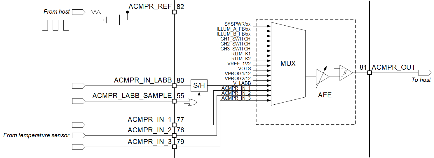
The measurement system (Figure 8-23) is designed to sense internal and external nodes and convert them to digital by the implemented AFE comparator. The reference signal for this comparator, ACMPR_REF, is a low pass filtered PWM signal coming from the DLPC. To be able to cover a wide range of input signals, a variable gain amplifier (VGA) is added with three gain settings (1x, 9.5x, and 18x). The maximum input voltage of the VGA is 1.5 V. However, some of the internal voltages are too large to be handled by the VGA and are divided down first.
 Figure 8-23 Measurement System
The system input voltage SYSPWR can be measured by selecting the SYSPWR/xx input of the MUX. Before the system input voltage is supplied to the MUX, the voltage needs to be divided. This is because the variable gain amplifier (VGA) can handle voltages up to 1.5 V, whereas the system voltage can be as high as 20 V. The division is done internally in the DLPA3000. The division factor selection (VIN division factor) is combined with the AUTO_LED_TURN_OFF functionality of the illumination driver.
The LED voltages can be monitored by measuring both the common anode of the LEDs as well as the cathode of each LED individually. The LED anode voltage (VLED) is measured by sensing the feedback pin of the illumination driver (ILLUM_A_FB). Like the SYSPWR, the LED anode voltage needs to be divided before feeding it to the MUX. The division factor is combined with the overvoltage fault level of the illumination driver. The cathode voltages CH1,2,3_SWITCH are fed directly to the MUX without division factor.
The LED current can be determined by knowing the value of sense resistor RLIM and the voltage across the resistor. The voltage at the top-side of the sense resistor can be measured by selecting MUX-input RLIM_K1. The bottom-side of the resistor is connected to GND.
VOTS is connected to an on-chip temperature sensor. The voltage is a measure for the junction temperature of the chip: Temperature (°C) = 300 × VOTS (V) –270,
LABB is a feature that is Local Area Brightness Boost. LABB increases the brightness locally while maintaining good contrast and saturation. The sensor needed for this feature should be connected to pin ACMPR_IN_LABB.
ACMPR_IN_1,2,3 can measure external signals from for instance a temperature sensor. It should be ensured that the voltage on the input does not exceed 1.5 V.