DLPS071A October   2015  – February 2023 DLPA3005

PRODUCTION DATA  

  1. Features
  2. Applications
  3. Description
  4. Revision History
  5. Pin Configuration and Functions
  6. Specifications
    1. 6.1 Absolute Maximum Ratings
    2. 6.2 ESD Ratings
    3. 6.3 Recommended Operating Conditions
    4. 6.4 Thermal Information
    5. 6.5 Electrical Characteristics
    6. 6.6 SPI Timing Parameters
  7. Detailed Description
    1. 7.1 Overview
    2. 7.2 Functional Block Description
    3. 7.3 Feature Description
      1. 7.3.1 Supply and Monitoring
        1. 7.3.1.1 Supply
        2. 7.3.1.2 Monitoring
          1. 7.3.1.2.1 Block Faults
          2. 7.3.1.2.2 Auto LED Turn Off Functionality
          3. 7.3.1.2.3 Thermal Protection
      2. 7.3.2 Illumination
        1. 7.3.2.1 Programmable Gain Block
        2. 7.3.2.2 LDO Illumination
        3. 7.3.2.3 Illumination Driver A
        4. 7.3.2.4 RGB Strobe Decoder
          1. 7.3.2.4.1 Break Before Make (BBM)
          2. 7.3.2.4.2 Openloop Voltage
          3. 7.3.2.4.3 Transient Current Limit
        5. 7.3.2.5 Illumination Monitoring
          1. 7.3.2.5.1 Power Good
          2. 7.3.2.5.2 Ratio Metric Overvoltage Protection
        6. 7.3.2.6 Illumination Driver plus Power FETs Efficiency
      3. 7.3.3 External Power FET Selection
        1. 7.3.3.1 Threshold Voltage
        2. 7.3.3.2 Gate Charge and Gate Timing
        3. 7.3.3.3 RDS(ON)
      4. 7.3.4 DMD Supplies
        1. 7.3.4.1 LDO DMD
        2. 7.3.4.2 DMD HV Regulator
        3. 7.3.4.3 DMD/DLPC Buck Converters
        4. 7.3.4.4 DMD Monitoring
          1. 7.3.4.4.1 Power Good
          2. 7.3.4.4.2 Overvoltage Fault
      5. 7.3.5 Buck Converters
        1. 7.3.5.1 LDO Bucks
        2. 7.3.5.2 General Purpose Buck Converter
        3. 7.3.5.3 Buck Converter Monitoring
          1. 7.3.5.3.1 Power Good
          2. 7.3.5.3.2 Overvoltage Fault
        4. 7.3.5.4 Buck Converter Efficiency
      6. 7.3.6 Auxiliary LDOs
      7. 7.3.7 Measurement System
    4. 7.4 Device Functional Modes
    5. 7.5 Programming
      1. 7.5.1 SPI
      2. 7.5.2 Interrupt
      3. 7.5.3 Fast-Shutdown in Case of Fault
      4. 7.5.4 Protected Registers
    6. 7.6 Register Maps
  8. Application and Implementation
    1. 8.1 Application Information
    2. 8.2 Typical Application
      1. 8.2.1 Design Requirements
      2. 8.2.2 Detailed Design Procedure
        1. 8.2.2.1 Component Selection for General-Purpose Buck Converters
      3. 8.2.3 Application Curve
    3. 8.3 System Example With DLPA3005 Internal Block Diagram
  9. Power Supply Recommendations
    1. 9.1 Power-Up and Power-Down Timing
  10. 10Layout
    1. 10.1 Layout Guidelines
      1. 10.1.1 SPI Connections
      2. 10.1.2 RLIM Routing
      3. 10.1.3 LED Connection
    2. 10.2 Layout Example
    3. 10.3 Thermal Considerations
  11. 11Device and Documentation Support
    1. 11.1 Device Support
      1. 11.1.1 Device Nomenclature
    2. 11.2 Third-Party Products Disclaimer
    3. 11.3 Related Links
    4. 11.4 Receiving Notification of Documentation Updates
    5. 11.5 Support Resources
    6. 11.6 Trademarks
    7. 11.7 Electrostatic Discharge Caution
    8. 11.8 Glossary
  12. 12Mechanical, Packaging, and Orderable Information
    1. 12.1 Package Option Addendum

Package Options

Mechanical Data (Package|Pins)
Thermal pad, mechanical data (Package|Pins)
Orderable Information

SPI Connections

The SPI interface consists of several digital lines and the SPI supply. If routing of the interface lines is not done properly, communication errors can occur. It should be prevented that SPI lines can pickup noise and possible interfering sources should be kept away from the interface.

Pickup of noise can be prevented by ensuring that the SPI ground line is routed together with the digital lines as much as possible to the respective pins. The SPI interface should be connected by a separate own ground connection to the DGND of the DLPA3005 (Figure 10-2). This prevents ground noise between SPI ground references of DLPA3005 and DLPC due to the high current in the system.
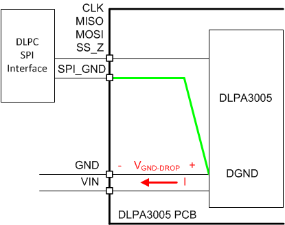
GUID-2B7AFCE9-CC9F-4432-A6F4-6A354E0CFD5D-low.gif Figure 10-2 SPI Connections

Interfering sources should be kept away from the interface lines as much as possible. If any power lines are routed too close to the SPI_CLK it could lead to false clock pulses and, thus, communication errors.