DLPS280 October   2024 DLPA3082

PRODUCTION DATA  

  1.   1
  2. Features
  3. Applications
  4. Description
  5. Pin Configuration and Functions
  6. Specifications
    1. 5.1 Absolute Maximum Ratings
    2. 5.2 ESD Ratings
    3. 5.3 Recommended Operating Conditions
    4. 5.4 Thermal Information
    5. 5.5 Electrical Characteristics
    6. 5.6 SPI Timing Parameters
  7. Detailed Description
    1. 6.1 Overview
    2. 6.2 Functional Block Description
    3. 6.3 Feature Description
      1. 6.3.1 Supply and Monitoring
        1. 6.3.1.1 Supply
        2. 6.3.1.2 Monitoring
          1. 6.3.1.2.1 Block Faults
          2. 6.3.1.2.2 Thermal Protection
      2. 6.3.2 DMD Supplies
        1. 6.3.2.1 LDO DMD
        2. 6.3.2.2 DMD HV Regulator
        3. 6.3.2.3 DMD/DLPC Buck Converters
        4. 6.3.2.4 DMD Monitoring
          1. 6.3.2.4.1 Power Good
          2. 6.3.2.4.2 Overvoltage Fault
      3. 6.3.3 Buck Converters
        1. 6.3.3.1 LDO Bucks
        2. 6.3.3.2 General Purpose Buck Converters
        3. 6.3.3.3 Buck Converter Monitoring
          1. 6.3.3.3.1 Power Good
          2. 6.3.3.3.2 Overvoltage Fault
        4. 6.3.3.4 Buck Converter Efficiency
      4. 6.3.4 Auxiliary LDOs
      5. 6.3.5 Measurement System
    4. 6.4 Device Functional Modes
    5. 6.5 Programming
      1. 6.5.1 SPI
      2. 6.5.2 Interrupt
      3. 6.5.3 Fast-Shutdown in Case of Fault
    6. 6.6 Register Maps
  8. Application and Implementation
    1. 7.1 Application Information
    2. 7.2 Typical Application
      1. 7.2.1 Design Requirements
      2. 7.2.2 Detailed Design Procedure
        1. 7.2.2.1 Component Selection for General-Purpose Buck Converter
    3. 7.3 System Example with DLPA3082 Internal Block Diagram
    4. 7.4 Power Supply Recommendations
      1. 7.4.1 Power-Up and Power-Down Timing
    5. 7.5 Layout
      1. 7.5.1 Layout Guidelines
        1. 7.5.1.1 SPI Connections
      2. 7.5.2 Layout Example
      3. 7.5.3 Thermal Considerations
  9. Device and Documentation Support
    1. 8.1 Third-Party Products Disclaimer
    2. 8.2 Device Support
      1. 8.2.1 Device Nomenclature
    3. 8.3 Receiving Notification of Documentation Updates
    4. 8.4 Support Resources
    5. 8.5 Trademarks
    6. 8.6 Electrostatic Discharge Caution
    7. 8.7 Glossary
  10. Revision History
  11. 10Mechanical, Packaging, and Orderable Information

Package Options

Mechanical Data (Package|Pins)
Thermal pad, mechanical data (Package|Pins)
Orderable Information

SPI Connections

The SPI interface consists of several digital lines and the SPI supply. If routing the interface lines is not done properly, communication errors can occur. Prevent SPI lines from picking up noise and keep other possible interfering sources from the interface.

Pickup of noise can be prevented by ensuring that the SPI ground line is routed together with the digital lines as much as possible to the respective pins. The SPI interface can be connected by a separate ground connection to the DGND of the DLPA3082 in Figure 7-6. This prevents ground noise between SPI ground references of DLPA3082 and DLPC due to the high current in the system.
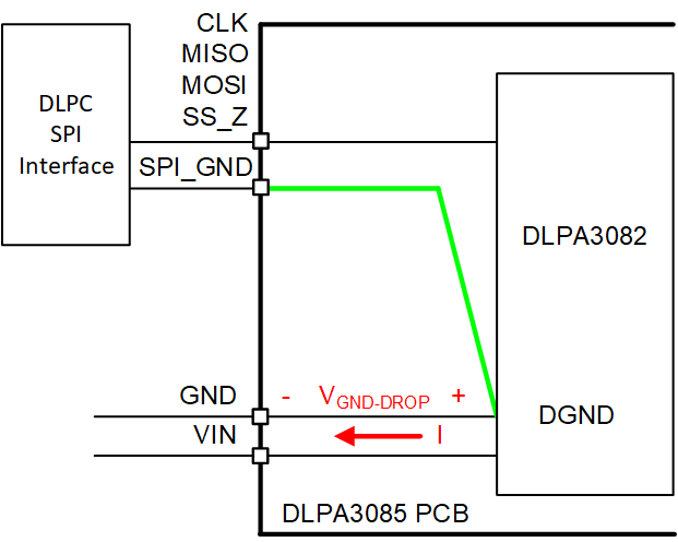
DLPA3082 SPI ConnectionsFigure 7-6 SPI Connections

Keep interfering sources away from the interface lines as much as possible. If any power lines are routed too close to the SPI_CLK, it can lead to false clock pulses and thus communication errors.