DLPS280 October   2024 DLPA3082

PRODUCTION DATA  

  1.   1
  2. Features
  3. Applications
  4. Description
  5. Pin Configuration and Functions
  6. Specifications
    1. 5.1 Absolute Maximum Ratings
    2. 5.2 ESD Ratings
    3. 5.3 Recommended Operating Conditions
    4. 5.4 Thermal Information
    5. 5.5 Electrical Characteristics
    6. 5.6 SPI Timing Parameters
  7. Detailed Description
    1. 6.1 Overview
    2. 6.2 Functional Block Description
    3. 6.3 Feature Description
      1. 6.3.1 Supply and Monitoring
        1. 6.3.1.1 Supply
        2. 6.3.1.2 Monitoring
          1. 6.3.1.2.1 Block Faults
          2. 6.3.1.2.2 Thermal Protection
      2. 6.3.2 DMD Supplies
        1. 6.3.2.1 LDO DMD
        2. 6.3.2.2 DMD HV Regulator
        3. 6.3.2.3 DMD/DLPC Buck Converters
        4. 6.3.2.4 DMD Monitoring
          1. 6.3.2.4.1 Power Good
          2. 6.3.2.4.2 Overvoltage Fault
      3. 6.3.3 Buck Converters
        1. 6.3.3.1 LDO Bucks
        2. 6.3.3.2 General Purpose Buck Converters
        3. 6.3.3.3 Buck Converter Monitoring
          1. 6.3.3.3.1 Power Good
          2. 6.3.3.3.2 Overvoltage Fault
        4. 6.3.3.4 Buck Converter Efficiency
      4. 6.3.4 Auxiliary LDOs
      5. 6.3.5 Measurement System
    4. 6.4 Device Functional Modes
    5. 6.5 Programming
      1. 6.5.1 SPI
      2. 6.5.2 Interrupt
      3. 6.5.3 Fast-Shutdown in Case of Fault
    6. 6.6 Register Maps
  8. Application and Implementation
    1. 7.1 Application Information
    2. 7.2 Typical Application
      1. 7.2.1 Design Requirements
      2. 7.2.2 Detailed Design Procedure
        1. 7.2.2.1 Component Selection for General-Purpose Buck Converter
    3. 7.3 System Example with DLPA3082 Internal Block Diagram
    4. 7.4 Power Supply Recommendations
      1. 7.4.1 Power-Up and Power-Down Timing
    5. 7.5 Layout
      1. 7.5.1 Layout Guidelines
        1. 7.5.1.1 SPI Connections
      2. 7.5.2 Layout Example
      3. 7.5.3 Thermal Considerations
  9. Device and Documentation Support
    1. 8.1 Third-Party Products Disclaimer
    2. 8.2 Device Support
      1. 8.2.1 Device Nomenclature
    3. 8.3 Receiving Notification of Documentation Updates
    4. 8.4 Support Resources
    5. 8.5 Trademarks
    6. 8.6 Electrostatic Discharge Caution
    7. 8.7 Glossary
  10. Revision History
  11. 10Mechanical, Packaging, and Orderable Information

Package Options

Mechanical Data (Package|Pins)
Thermal pad, mechanical data (Package|Pins)
Orderable Information

Measurement System

The measurement system (Figure 6-8) is designed to sense internal and external nodes and convert them to digital by the implemented AFE comparator. The reference signal for this comparator, ACMPR_REF, is a low-pass filtered PWM signal coming from the DLPC. To be able to cover a wide range of input signals, a variable gain amplifier (VGA) is added with three gain settings (1x, 9.5x, and 18x). The maximum input voltage of the VGA is 1.5V. However, some of the internal voltages are too large to be handled by the VGA and are divided down first.
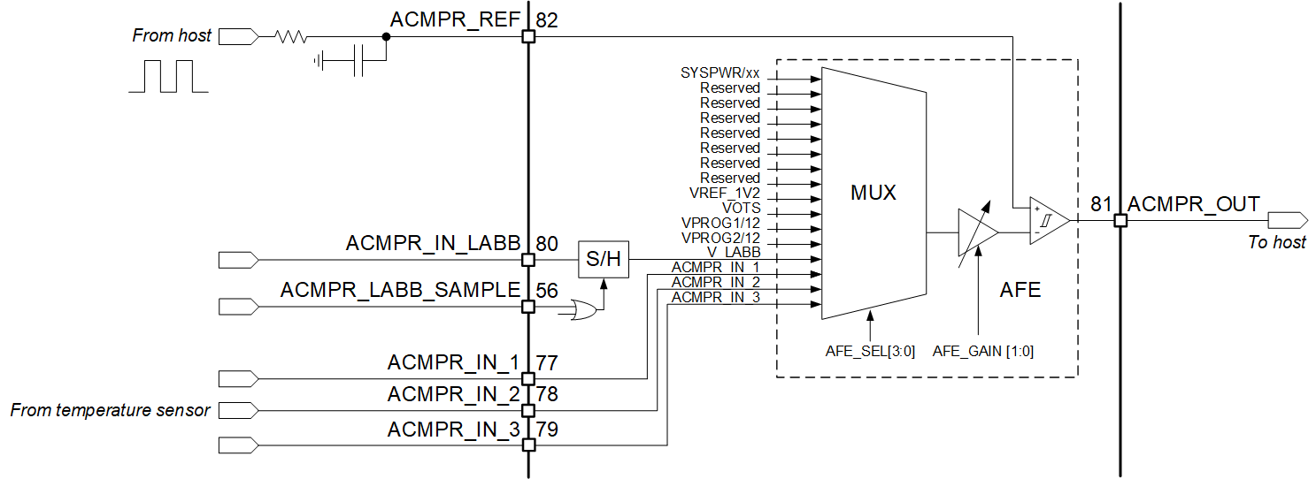
DLPA3082 Measurement System SchematicFigure 6-8 Measurement System Schematic

The system input voltage SYSPWR can be measured by selecting the SYSPWR/xx input of the MUX. Before the system input voltage is supplied to the MUX, the voltage needs to be divided. This is because the variable gain amplifier (VGA) can handle voltages up to 1.5V, whereas the system voltage can be as high as 20V. The division is done internally in the DLPA3082.

VOTS is connected to an on-chip temperature sensor. The voltage is a measure of the chip’s junction temperature: Temperature (°C) = 300 × VOTS (V) – 270.

LABB is a feature that stands for Local Area Brightness Boost. LABB locally increases the brightness while maintaining good contrast and saturation. Connect the sensor this feature to pin ACMPR_IN_LABB.

ACMPR_IN_1,2,3 can measure external signals from for instance a temperature sensor. Ensure the voltage on the input does not exceed 1.5V.