DLPS280 October   2024 DLPA3082

PRODUCTION DATA  

  1.   1
  2. Features
  3. Applications
  4. Description
  5. Pin Configuration and Functions
  6. Specifications
    1. 5.1 Absolute Maximum Ratings
    2. 5.2 ESD Ratings
    3. 5.3 Recommended Operating Conditions
    4. 5.4 Thermal Information
    5. 5.5 Electrical Characteristics
    6. 5.6 SPI Timing Parameters
  7. Detailed Description
    1. 6.1 Overview
    2. 6.2 Functional Block Description
    3. 6.3 Feature Description
      1. 6.3.1 Supply and Monitoring
        1. 6.3.1.1 Supply
        2. 6.3.1.2 Monitoring
          1. 6.3.1.2.1 Block Faults
          2. 6.3.1.2.2 Thermal Protection
      2. 6.3.2 DMD Supplies
        1. 6.3.2.1 LDO DMD
        2. 6.3.2.2 DMD HV Regulator
        3. 6.3.2.3 DMD/DLPC Buck Converters
        4. 6.3.2.4 DMD Monitoring
          1. 6.3.2.4.1 Power Good
          2. 6.3.2.4.2 Overvoltage Fault
      3. 6.3.3 Buck Converters
        1. 6.3.3.1 LDO Bucks
        2. 6.3.3.2 General Purpose Buck Converters
        3. 6.3.3.3 Buck Converter Monitoring
          1. 6.3.3.3.1 Power Good
          2. 6.3.3.3.2 Overvoltage Fault
        4. 6.3.3.4 Buck Converter Efficiency
      4. 6.3.4 Auxiliary LDOs
      5. 6.3.5 Measurement System
    4. 6.4 Device Functional Modes
    5. 6.5 Programming
      1. 6.5.1 SPI
      2. 6.5.2 Interrupt
      3. 6.5.3 Fast-Shutdown in Case of Fault
    6. 6.6 Register Maps
  8. Application and Implementation
    1. 7.1 Application Information
    2. 7.2 Typical Application
      1. 7.2.1 Design Requirements
      2. 7.2.2 Detailed Design Procedure
        1. 7.2.2.1 Component Selection for General-Purpose Buck Converter
    3. 7.3 System Example with DLPA3082 Internal Block Diagram
    4. 7.4 Power Supply Recommendations
      1. 7.4.1 Power-Up and Power-Down Timing
    5. 7.5 Layout
      1. 7.5.1 Layout Guidelines
        1. 7.5.1.1 SPI Connections
      2. 7.5.2 Layout Example
      3. 7.5.3 Thermal Considerations
  9. Device and Documentation Support
    1. 8.1 Third-Party Products Disclaimer
    2. 8.2 Device Support
      1. 8.2.1 Device Nomenclature
    3. 8.3 Receiving Notification of Documentation Updates
    4. 8.4 Support Resources
    5. 8.5 Trademarks
    6. 8.6 Electrostatic Discharge Caution
    7. 8.7 Glossary
  10. Revision History
  11. 10Mechanical, Packaging, and Orderable Information

Package Options

Mechanical Data (Package|Pins)
Thermal pad, mechanical data (Package|Pins)
Orderable Information

Description

The DLPA3082 is a highly-integrated power management IC optimized for DLP®Pico™ Projector systems. The DLPA3082 contains five buck converters, two of which are dedicated for DLPC low voltage supplies. Another dedicated regulating supply generates the three timing-critical DC supplies for the DMD: VBIAS, VRST, and VOFS.

The DLPA3082 contains several auxiliary blocks which are used in a flexible way. This enables a tailor-made Pico Projector system. One 8-bit programmable buck converter isused, for instance, to make auxiliary supply line. General purpose buck2 (PWR6) is currently supported. Two LDOs are used for a lower-current supply, up to 200mA. These LDOs are predefined to 2.5V and 3.3V.

Through the SPI, all blocks of the DLPA3082 are addressed. Features included are the generation of the system reset, power sequencing, IC self-protections, and an analog MUX for routing analog information to an external ADC.

Device Information
PART NUMBER PACKAGE PACKAGE SIZE
DLPA3082(1) HTQFP (100) 14.00mm × 14.00mm
For more information, see the Mechanical, Packaging, and Orderable addendum.
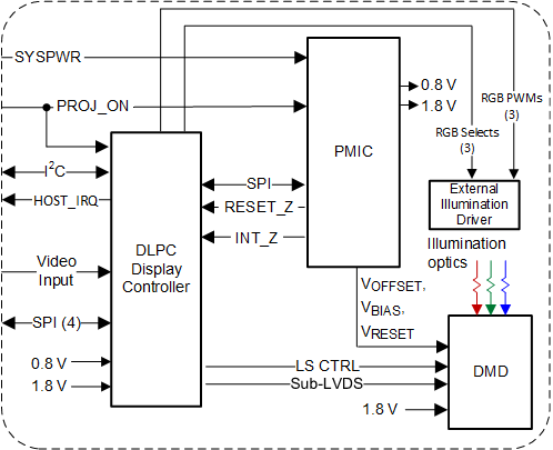
DLPA3082 Typical Simplified System Typical Simplified System