DLPS280 October 2024 DLPA3082
PRODUCTION DATA
- 1
- 1 Features
- 2 Applications
- 3 Description
- 4 Pin Configuration and Functions
- 5 Specifications
- 6 Detailed Description
- 7 Application and Implementation
- 8 Device and Documentation Support
- 9 Revision History
- 10Mechanical, Packaging, and Orderable Information
Package Options
Mechanical Data (Package|Pins)
- PFD|100
Thermal pad, mechanical data (Package|Pins)
- PFD|100
Orderable Information
6.3.1.1 Supply
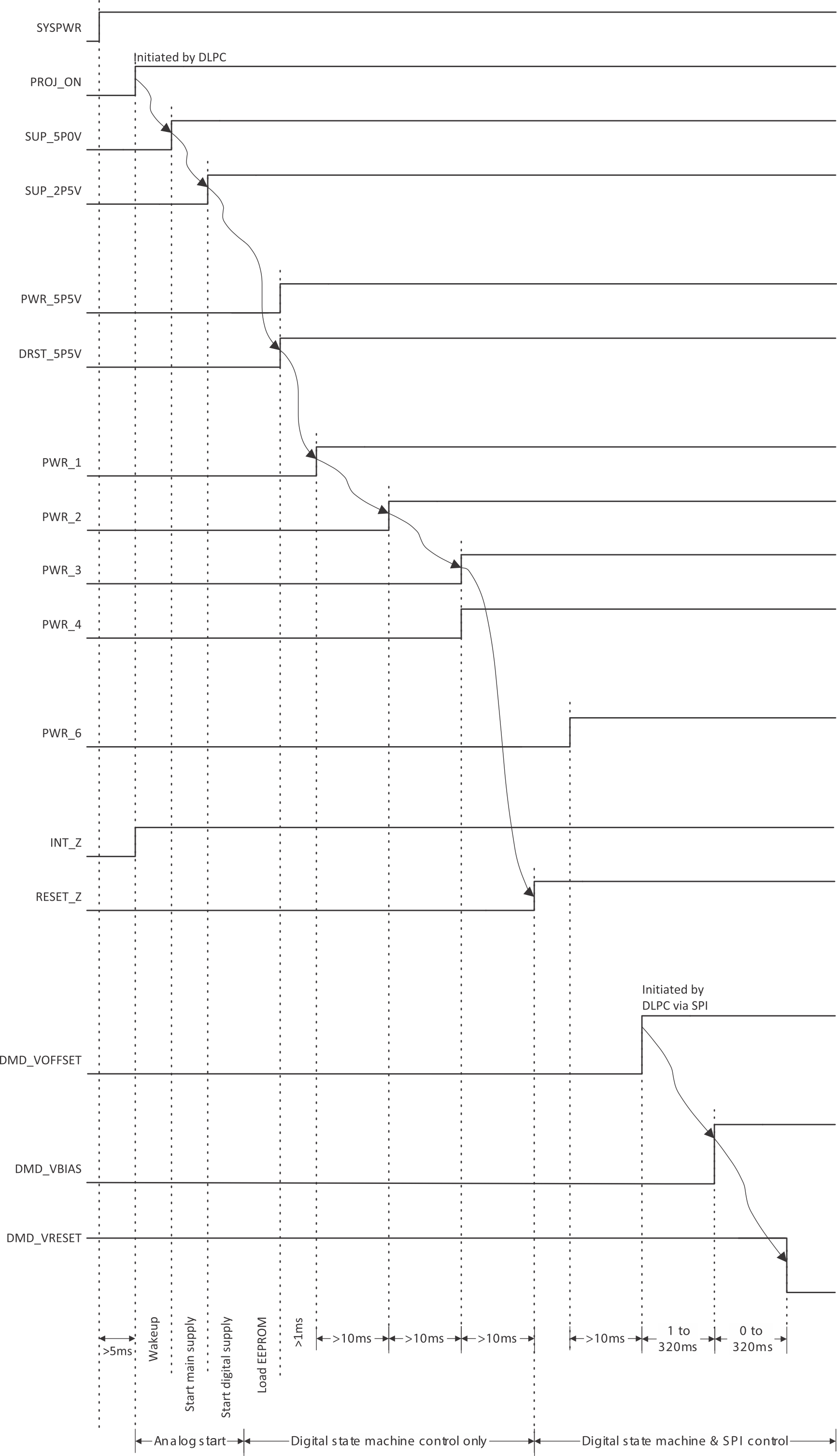
SYSPWR is the main supply of the DLPA3082. It ranges from 6V to 20V, where the typical is 12V. At power-up, several (internal) power supplies are started one after the other to make the system work correctly (Figure 6-1). A sequential startup ensures that all the different blocks start in a certain order and prevent excessive startup currents. The main control to start the DLPA3082 is the control pin PROJ_ON. Once set high the basic analog circuitry is started that is needed to operate the digital and SPI interface. This circuitry is supplied by two LDO regulators that generate 2.5V (SUP_2P5V) and 5V (SUP_5P0V). These regulator voltages are for internal use only and cannot be loaded by an external application. The output capacitors of those LDOs can be 2.2µF for the 2.5V LDO, and 4.7µF for the 5V LDO, pin 91 and 92, respectively. Once these are up the digital core is started, and the DLPA3082 Digital State Machine (DSM) takes over.
Subsequently, the 5.5V LDOs for various blocks are started: PWR_5P5V and DRST_5P5V. Next, the buck converters and DMD LDOs are started (PWR_1 to PWR_4). The DLPA30085 is now awake and ready to be controlled by the DLPC (indicated by RESET_Z going high).
The general purpose buck converter (PWR_6) can be started (if used) as well as the regulator that supplies the DMD. The DMD regulator generates the timing critical VOFFSET, VBIAS, and VRESET supplies.

- Arrows indicate the sequence of events automatically controlled by the digital state machine. Other events are initiated under SPI control.
- SUP_5P0V and SUP_2P5V rise to a precharge level with SYSPWR, and reach the full level potential after PROJ_ON is pulled high.