DLPS240A June   2024  – August 2024 DLPA3085

PRODUCTION DATA  

  1.   1
  2. Features
  3. Applications
  4. Description
  5. Pin Configuration and Functions
  6. Specifications
    1. 5.1 Absolute Maximum Ratings
    2. 5.2 ESD Ratings
    3. 5.3 Recommended Operating Conditions
    4. 5.4 Thermal Information
    5. 5.5 Electrical Characteristics
    6. 5.6 SPI Timing Parameters
  7. Detailed Description
    1. 6.1 Overview
    2. 6.2 Functional Block Description
    3. 6.3 Feature Description
      1. 6.3.1 Supply and Monitoring
        1. 6.3.1.1 Supply
        2. 6.3.1.2 Monitoring
          1. 6.3.1.2.1 Block Faults
          2. 6.3.1.2.2 Auto LED Turn-Off Functionality
          3. 6.3.1.2.3 Thermal Protection
      2. 6.3.2 Illumination
        1. 6.3.2.1 Programmable Gain Block
        2. 6.3.2.2 LDO Illumination
        3. 6.3.2.3 Illumination Driver A
        4. 6.3.2.4 RGB Strobe Decoder
          1. 6.3.2.4.1 Break Before Make (BBM)
          2. 6.3.2.4.2 Openloop Voltage
          3. 6.3.2.4.3 Transient Current Limit
        5. 6.3.2.5 Illumination Monitoring
          1. 6.3.2.5.1 Power Good
          2. 6.3.2.5.2 Ratio Metric Overvoltage Protection
        6. 6.3.2.6 Illumination Driver Plus Power FETs Efficiency
      3. 6.3.3 External Power FET Selection
        1. 6.3.3.1 Threshold Voltage
        2. 6.3.3.2 Gate Charge and Gate Timing
        3. 6.3.3.3 RDS(ON)
      4. 6.3.4 DMD Supplies
        1. 6.3.4.1 LDO DMD
        2. 6.3.4.2 DMD HV Regulator
        3. 6.3.4.3 DMD/DLPC Buck Converters
        4. 6.3.4.4 DMD Monitoring
          1. 6.3.4.4.1 Power Good
          2. 6.3.4.4.2 Overvoltage Fault
      5. 6.3.5 Buck Converters
        1. 6.3.5.1 LDO Bucks
        2. 6.3.5.2 General Purpose Buck Converters
        3. 6.3.5.3 Buck Converter Monitoring
          1. 6.3.5.3.1 Power Good
          2. 6.3.5.3.2 Overvoltage Fault
        4. 6.3.5.4 Buck Converter Efficiency
      6. 6.3.6 Auxiliary LDOs
      7. 6.3.7 Measurement System
    4. 6.4 Device Functional Modes
    5. 6.5 Programming
      1. 6.5.1 SPI
      2. 6.5.2 Interrupt
      3. 6.5.3 Fast-Shutdown in Case of Fault
    6. 6.6 Register Maps
  8. Application and Implementation
    1. 7.1 Application Information
    2. 7.2 Typical Application
      1. 7.2.1 Design Requirements
      2. 7.2.2 Detailed Design Procedure
        1. 7.2.2.1 Component Selection for General-Purpose Buck Converter
      3. 7.2.3 Application Curve
    3. 7.3 System Example With DLPA3085 Internal Block Diagram
  9. Power Supply Recommendations
    1. 8.1 Power-Up and Power-Down Timing
  10. Layout
    1. 9.1 Layout Guidelines
      1. 9.1.1 SPI Connections
      2. 9.1.2 RLIM Routing
      3. 9.1.3 LED Connection
    2. 9.2 Layout Example
    3. 9.3 Thermal Considerations
  11. 10Device and Documentation Support
    1. 10.1 Third-Party Products Disclaimer
    2. 10.2 Device Support
      1. 10.2.1 Device Nomenclature
    3. 10.3 Receiving Notification of Documentation Updates
    4. 10.4 Support Resources
    5. 10.5 Trademarks
    6. 10.6 Electrostatic Discharge Caution
    7. 10.7 Glossary
  12. 11Revision History
  13. 12Mechanical, Packaging, and Orderable Information

Package Options

Mechanical Data (Package|Pins)
Thermal pad, mechanical data (Package|Pins)
Orderable Information

Buck Converters

The DLPA3085 contains one general purpose buck converter and a supporting LDO (LDO_BUCKS). The programmable 8-bit buck converter can generate a voltage between 1V and 5V and have an output current limit of 3A. General purpose buck2 (PWR6) is currently supported. One buck converter and the LDO_BUCKS are depicted in Figure 6-15.

The two DMD/DLPC buck converters discussed earlier in Section 6.3.4 have the same architecture as the buck converter and can be configured in the same way.
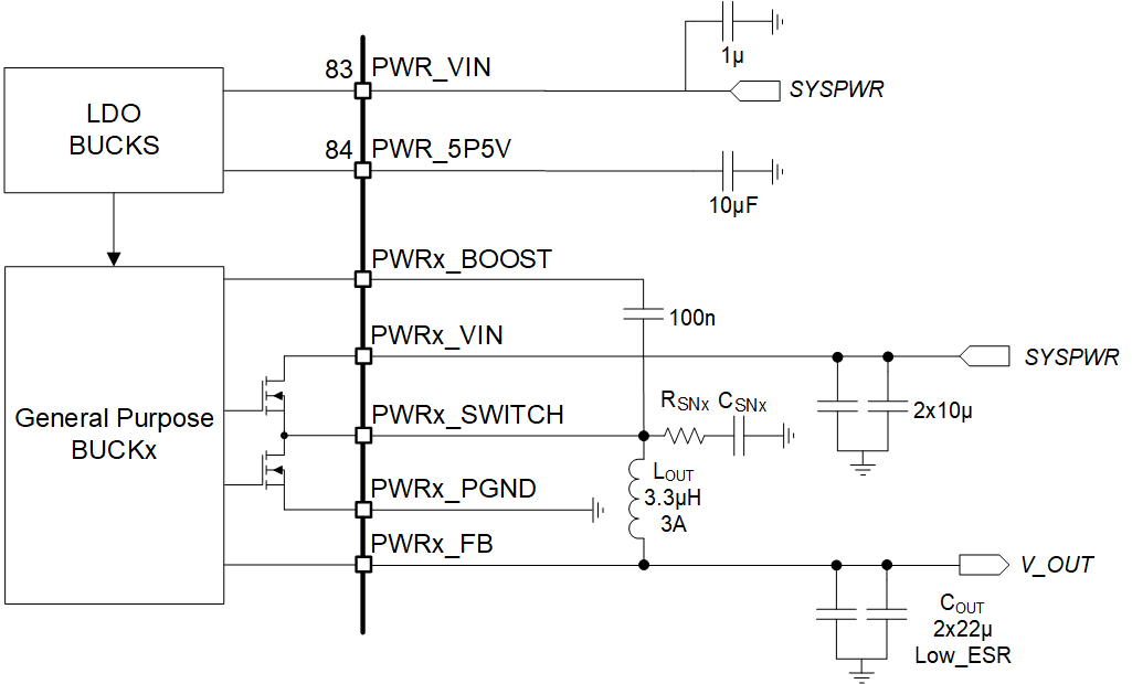
DLPA3085 Buck
                    Converter Figure 6-15 Buck Converter