DLPS240A June   2024  – August 2024 DLPA3085

PRODUCTION DATA  

  1.   1
  2. Features
  3. Applications
  4. Description
  5. Pin Configuration and Functions
  6. Specifications
    1. 5.1 Absolute Maximum Ratings
    2. 5.2 ESD Ratings
    3. 5.3 Recommended Operating Conditions
    4. 5.4 Thermal Information
    5. 5.5 Electrical Characteristics
    6. 5.6 SPI Timing Parameters
  7. Detailed Description
    1. 6.1 Overview
    2. 6.2 Functional Block Description
    3. 6.3 Feature Description
      1. 6.3.1 Supply and Monitoring
        1. 6.3.1.1 Supply
        2. 6.3.1.2 Monitoring
          1. 6.3.1.2.1 Block Faults
          2. 6.3.1.2.2 Auto LED Turn-Off Functionality
          3. 6.3.1.2.3 Thermal Protection
      2. 6.3.2 Illumination
        1. 6.3.2.1 Programmable Gain Block
        2. 6.3.2.2 LDO Illumination
        3. 6.3.2.3 Illumination Driver A
        4. 6.3.2.4 RGB Strobe Decoder
          1. 6.3.2.4.1 Break Before Make (BBM)
          2. 6.3.2.4.2 Openloop Voltage
          3. 6.3.2.4.3 Transient Current Limit
        5. 6.3.2.5 Illumination Monitoring
          1. 6.3.2.5.1 Power Good
          2. 6.3.2.5.2 Ratio Metric Overvoltage Protection
        6. 6.3.2.6 Illumination Driver Plus Power FETs Efficiency
      3. 6.3.3 External Power FET Selection
        1. 6.3.3.1 Threshold Voltage
        2. 6.3.3.2 Gate Charge and Gate Timing
        3. 6.3.3.3 RDS(ON)
      4. 6.3.4 DMD Supplies
        1. 6.3.4.1 LDO DMD
        2. 6.3.4.2 DMD HV Regulator
        3. 6.3.4.3 DMD/DLPC Buck Converters
        4. 6.3.4.4 DMD Monitoring
          1. 6.3.4.4.1 Power Good
          2. 6.3.4.4.2 Overvoltage Fault
      5. 6.3.5 Buck Converters
        1. 6.3.5.1 LDO Bucks
        2. 6.3.5.2 General Purpose Buck Converters
        3. 6.3.5.3 Buck Converter Monitoring
          1. 6.3.5.3.1 Power Good
          2. 6.3.5.3.2 Overvoltage Fault
        4. 6.3.5.4 Buck Converter Efficiency
      6. 6.3.6 Auxiliary LDOs
      7. 6.3.7 Measurement System
    4. 6.4 Device Functional Modes
    5. 6.5 Programming
      1. 6.5.1 SPI
      2. 6.5.2 Interrupt
      3. 6.5.3 Fast-Shutdown in Case of Fault
    6. 6.6 Register Maps
  8. Application and Implementation
    1. 7.1 Application Information
    2. 7.2 Typical Application
      1. 7.2.1 Design Requirements
      2. 7.2.2 Detailed Design Procedure
        1. 7.2.2.1 Component Selection for General-Purpose Buck Converter
      3. 7.2.3 Application Curve
    3. 7.3 System Example With DLPA3085 Internal Block Diagram
  9. Power Supply Recommendations
    1. 8.1 Power-Up and Power-Down Timing
  10. Layout
    1. 9.1 Layout Guidelines
      1. 9.1.1 SPI Connections
      2. 9.1.2 RLIM Routing
      3. 9.1.3 LED Connection
    2. 9.2 Layout Example
    3. 9.3 Thermal Considerations
  11. 10Device and Documentation Support
    1. 10.1 Third-Party Products Disclaimer
    2. 10.2 Device Support
      1. 10.2.1 Device Nomenclature
    3. 10.3 Receiving Notification of Documentation Updates
    4. 10.4 Support Resources
    5. 10.5 Trademarks
    6. 10.6 Electrostatic Discharge Caution
    7. 10.7 Glossary
  12. 11Revision History
  13. 12Mechanical, Packaging, and Orderable Information

Package Options

Mechanical Data (Package|Pins)
Thermal pad, mechanical data (Package|Pins)
Orderable Information
Ratio Metric Overvoltage Protection

The DLPA3085 illumination driver LED outputs are protected against open circuit use. In case no LED is connected and the DLPA3085 is instructed to set the LED current to a specific level, the LED voltage (ILLUM_A_FB) quickly rises and potentially rails to VIN; however, the OVP protection circuit triggers once VLED crosses a predefined level. As a result, the DLPA3085 is switched off, preventing overvoltage from occurring.

The same protection circuit is triggered in case the supply voltage (VINA) becomes too low for the DLPA3085 to work properly given the VLED level. This protection circuit is constructed around a comparator that senses both the LED voltage and the VINA supply voltage. The fraction of the VINA is connected to the minus input of the comparator while the fraction of the VLED voltage is connected to the plus input. Triggering occurs when the plus input rises above the minus input and an OVP fault is set. The fraction of the VINA must be set between 1V and 4V to ensure proper operation of the comparator.
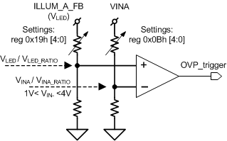
DLPA3085 Ratio
                    Metric OVP Figure 6-9 Ratio Metric OVP

In general, an OVP fault is set when the following occurs:

VLED/VLED_RATIO ≥ VINA/VINA_RATIO
thus when:
VLED ≥ VINA × VLED_RATIO/VINA_RATIO.