DLPS240A June 2024 – August 2024 DLPA3085
PRODUCTION DATA
- 1
- 1 Features
- 2 Applications
- 3 Description
- 4 Pin Configuration and Functions
- 5 Specifications
-
6 Detailed Description
- 6.1 Overview
- 6.2 Functional Block Description
- 6.3
Feature Description
- 6.3.1 Supply and Monitoring
- 6.3.2 Illumination
- 6.3.3 External Power FET Selection
- 6.3.4 DMD Supplies
- 6.3.5 Buck Converters
- 6.3.6 Auxiliary LDOs
- 6.3.7 Measurement System
- 6.4 Device Functional Modes
- 6.5 Programming
- 6.6 Register Maps
- 7 Application and Implementation
- 8 Power Supply Recommendations
- 9 Layout
- 10Device and Documentation Support
- 11Revision History
- 12Mechanical, Packaging, and Orderable Information
Package Options
Mechanical Data (Package|Pins)
- PFD|100
Thermal pad, mechanical data (Package|Pins)
- PFD|100
Orderable Information
6.3.2.4 RGB Strobe Decoder
The DLPA3085 contains circuitry to sequentially control the three color-LEDs (red, green, and blue). This circuitry consists of three drivers to control external switches, the actual strobe decoder and the LED current control (Figure 6-6). The NMOS switches are connected to the cathode terminals of the external LED package and turn on and off the currents through the LEDs.
 Figure 6-6 Switch
Connection for a Common-Anode LED Assembly
Figure 6-6 Switch
Connection for a Common-Anode LED AssemblyThe NMOS FETs P, Q, and R are controlled by the CH_SEL_0 and CH_SEL_1 pins. CH_SEL[1:0] typically receives rotating code-switching from RED to GREEN to BLUE and then back to RED. The relation between CH_SEL[0:1] and which switch is closed is indicated in Table 6-1.
| PINS CH_SEL[1:0] | SWITCH | IDAC REGISTER | ||
|---|---|---|---|---|
| P | Q | R | ||
| 00 | Open | Open | Open | N/A |
| 01 | Closed | Open | Open | 0x03 and 0x04 SW1_IDAC[9:0] |
| 10 | Open | Closed | Open | 0x05 and 0x06 SW2_IDAC[9:0] |
| 11 | Open | Open | Closed | 0x07 and 0x08 SW3_IDAC[9:0] |
Besides enabling one of the switches, CH_SEL[1:0] also selects a 10-bit current setting for the control IDAC that is used as the set current for the LED. This set current, together with the measured current through RLIM, controls the illumination driver to the appropriate VLED. The current through the three LEDs can be set independently by registers SW1_IDAC to SW3_IDAC, 0x03 to 0x08 (Table 6-1).
Each current level can be set from off to 150mV/RLIM in 1023 steps:
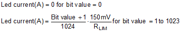
For single LED, the maximum current for RLIM= 9.4mΩ is thus 16A.
For two LEDs in series, the maximum current is 32A, thus RLIM (for example, RLIM= 4.7mΩ to support configuration for 32A) needs to change for a higher LED current.
For proper operation a minimum LED current of 5% of ILED_MAX is required.