DLPS240A June   2024  – August 2024 DLPA3085

PRODUCTION DATA  

  1.   1
  2. Features
  3. Applications
  4. Description
  5. Pin Configuration and Functions
  6. Specifications
    1. 5.1 Absolute Maximum Ratings
    2. 5.2 ESD Ratings
    3. 5.3 Recommended Operating Conditions
    4. 5.4 Thermal Information
    5. 5.5 Electrical Characteristics
    6. 5.6 SPI Timing Parameters
  7. Detailed Description
    1. 6.1 Overview
    2. 6.2 Functional Block Description
    3. 6.3 Feature Description
      1. 6.3.1 Supply and Monitoring
        1. 6.3.1.1 Supply
        2. 6.3.1.2 Monitoring
          1. 6.3.1.2.1 Block Faults
          2. 6.3.1.2.2 Auto LED Turn-Off Functionality
          3. 6.3.1.2.3 Thermal Protection
      2. 6.3.2 Illumination
        1. 6.3.2.1 Programmable Gain Block
        2. 6.3.2.2 LDO Illumination
        3. 6.3.2.3 Illumination Driver A
        4. 6.3.2.4 RGB Strobe Decoder
          1. 6.3.2.4.1 Break Before Make (BBM)
          2. 6.3.2.4.2 Openloop Voltage
          3. 6.3.2.4.3 Transient Current Limit
        5. 6.3.2.5 Illumination Monitoring
          1. 6.3.2.5.1 Power Good
          2. 6.3.2.5.2 Ratio Metric Overvoltage Protection
        6. 6.3.2.6 Illumination Driver Plus Power FETs Efficiency
      3. 6.3.3 External Power FET Selection
        1. 6.3.3.1 Threshold Voltage
        2. 6.3.3.2 Gate Charge and Gate Timing
        3. 6.3.3.3 RDS(ON)
      4. 6.3.4 DMD Supplies
        1. 6.3.4.1 LDO DMD
        2. 6.3.4.2 DMD HV Regulator
        3. 6.3.4.3 DMD/DLPC Buck Converters
        4. 6.3.4.4 DMD Monitoring
          1. 6.3.4.4.1 Power Good
          2. 6.3.4.4.2 Overvoltage Fault
      5. 6.3.5 Buck Converters
        1. 6.3.5.1 LDO Bucks
        2. 6.3.5.2 General Purpose Buck Converters
        3. 6.3.5.3 Buck Converter Monitoring
          1. 6.3.5.3.1 Power Good
          2. 6.3.5.3.2 Overvoltage Fault
        4. 6.3.5.4 Buck Converter Efficiency
      6. 6.3.6 Auxiliary LDOs
      7. 6.3.7 Measurement System
    4. 6.4 Device Functional Modes
    5. 6.5 Programming
      1. 6.5.1 SPI
      2. 6.5.2 Interrupt
      3. 6.5.3 Fast-Shutdown in Case of Fault
    6. 6.6 Register Maps
  8. Application and Implementation
    1. 7.1 Application Information
    2. 7.2 Typical Application
      1. 7.2.1 Design Requirements
      2. 7.2.2 Detailed Design Procedure
        1. 7.2.2.1 Component Selection for General-Purpose Buck Converter
      3. 7.2.3 Application Curve
    3. 7.3 System Example With DLPA3085 Internal Block Diagram
  9. Power Supply Recommendations
    1. 8.1 Power-Up and Power-Down Timing
  10. Layout
    1. 9.1 Layout Guidelines
      1. 9.1.1 SPI Connections
      2. 9.1.2 RLIM Routing
      3. 9.1.3 LED Connection
    2. 9.2 Layout Example
    3. 9.3 Thermal Considerations
  11. 10Device and Documentation Support
    1. 10.1 Third-Party Products Disclaimer
    2. 10.2 Device Support
      1. 10.2.1 Device Nomenclature
    3. 10.3 Receiving Notification of Documentation Updates
    4. 10.4 Support Resources
    5. 10.5 Trademarks
    6. 10.6 Electrostatic Discharge Caution
    7. 10.7 Glossary
  12. 11Revision History
  13. 12Mechanical, Packaging, and Orderable Information

Package Options

Mechanical Data (Package|Pins)
Thermal pad, mechanical data (Package|Pins)
Orderable Information

RDS(ON)

Selecting the FET relative to its drain-source on-resistance, RDS(ON) has two aspects. First, for the high-side FET of the illumination buck-converter, the RDS(ON) is a factor in the overcurrent detection. Second, for the other four FETs, the power dissipation drives the choice of the FETs RDS(ON).

To detect an overcurrent situation, the DLPA3085 measures the drain-source voltage drop of the high-side FET when turned on. The overcurrent detection circuit triggers and switches off the high-side FET when the threshold VDC-Th = 185mV (typical) is reached. Therefore, the actual current, IOC, at which this overcurrent detection triggers is given by:

Equation 6. DLPA3085
Note: Take the RDS(ON) from the FET data sheet at high-temp; that is, at overcurrent the FETs are likely hot.

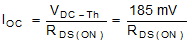
For example, the CSD17510Q5A NexFET has an RDS(ON) of 7mΩ at 125 °C. Using this FET results in an overcurrent level of 26A. This FET would be a good choice for a 16A application.

For the low-side FET and the three LED selection FETs, the RDS(ON) selection is mainly governed by the power dissipation due to conduction losses. The power dissipated in these FETs is given by:

Equation 7. DLPA3085

IDS is the current running through the respective FET. The lower the RDS(ON), the lower the dissipation. For example, the CSD17501Q5A has RDS(ON)= 3mΩ. For a drain-source current of 16A with a duty cycle of 25% (assuming the FET is used as LED selection switch), the dissipation is about 0.2W in this FET.