DLPS240A June 2024 – August 2024 DLPA3085
PRODUCTION DATA
- 1
- 1 Features
- 2 Applications
- 3 Description
- 4 Pin Configuration and Functions
- 5 Specifications
-
6 Detailed Description
- 6.1 Overview
- 6.2 Functional Block Description
- 6.3
Feature Description
- 6.3.1 Supply and Monitoring
- 6.3.2 Illumination
- 6.3.3 External Power FET Selection
- 6.3.4 DMD Supplies
- 6.3.5 Buck Converters
- 6.3.6 Auxiliary LDOs
- 6.3.7 Measurement System
- 6.4 Device Functional Modes
- 6.5 Programming
- 6.6 Register Maps
- 7 Application and Implementation
- 8 Power Supply Recommendations
- 9 Layout
- 10Device and Documentation Support
- 11Revision History
- 12Mechanical, Packaging, and Orderable Information
Package Options
Mechanical Data (Package|Pins)
- PFD|100
Thermal pad, mechanical data (Package|Pins)
- PFD|100
Orderable Information
9.1.3 LED Connection
High switching currents run through the wiring connecting the external RGB switches and the LEDs; therefore, this needs special attention. Two perspectives apply to the LED-to-RGB switches wiring:
- The resistance of the wiring, Rseries
- The inductance of the wiring, Lseries
The location of the parasitic series impedances is depicted in Figure 9-3.
 and Resistance (Rseries) in Series with LED") Figure 9-3 Parasitic Inductance (LSeries) and Resistance (Rseries) in Series with LED
Figure 9-3 Parasitic Inductance (LSeries) and Resistance (Rseries) in Series with LEDCurrents up to 16A can run through the wires connecting the LEDs to the RGB switches. Some noticeable dissipation can be caused. Every 10mΩ of series resistances implies for 16A average LED current a parasitic power dissipation of 2.5W. This might cause PCB heating, but more importantly, overall system efficiency deteriorates.
Additionally, the resistance of the wiring might impact the control dynamics of the LED current. It should be noted that the routing resistance is part of the LED current control loop. The LED current is controlled by VLED. For a small change in VLED (ΔVLED), the resulting LED current variation (ΔILED) is given by the total differential resistance in that path, as:
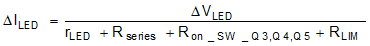
- rLED is the differential resistance of the LED.
- Ron_SW_P,Q,R the on-resistance of the strobe decoder switch.
In this expression, Lseries is ignored because realistic values are usually sufficiently low to cause any noticeable impact on the dynamics.
All the comprising differential resistances are in the range of 12.5mΩ to several 100mΩ. Without paying special attention, a series resistance of 100mΩ can easily be obtained. It is advised to keep this series resistance sufficiently low; that is, <10mΩ.
The series inductance plays an important role when considering the switched nature of the LED current. While cycling through R, G, and B LEDs, the current through these branches is turned on and turned off in short time duration. Specifically turning off is fast. A current of 16A goes to 0A in a matter of 50ns. This implies a voltage spike of about 1V for every 5nH of parasitic inductance. Minimize the series inductance of the LED wiring with the following:
- Short wires
- Thick wires / multiple parallel wires
- The small enclosed area of the forward and return current path
If the inductance cannot be made sufficiently low, use a Zener diode to clamp the drain voltage of the RGB switch so it does not surpass the absolute maximum rating. Choose the clamping voltage between the maximum expected VLED and the absolute maximum rating. Ensure a sufficient margin of the clamping voltage relative to the mentioned minimum and maximum voltage.