DLPS132 May   2018 DLPA4000

PRODUCTION DATA.  

  1. Features
  2. Applications
  3. Description
    1.     Device Images
      1.      System Block Diagram
  4. Revision History
  5. Pin Configuration and Functions
    1.     Pin Functions
  6. Specifications
    1. 6.1 Absolute Maximum Ratings
    2. 6.2 ESD Ratings
    3. 6.3 Recommended Operating Conditions
    4. 6.4 Thermal Information
    5. 6.5 Electrical Characteristics
    6. 6.6 SPI Timing Parameters
  7. Detailed Description
    1. 7.1 Overview
    2. 7.2 Functional Block Description
    3. 7.3 Feature Description
      1. 7.3.1 Supply and Monitoring
        1. 7.3.1.1 Supply
        2. 7.3.1.2 Monitoring
          1. 7.3.1.2.1 Block Faults
          2. 7.3.1.2.2 Low Battery and UVLO
          3. 7.3.1.2.3 Thermal Protection
      2. 7.3.2 Illumination
        1. 7.3.2.1 Programmable Gain Block
        2. 7.3.2.2 LDO Illumination
        3. 7.3.2.3 Illumination Driver A
        4. 7.3.2.4 External MOSFETs
          1. 7.3.2.4.1 Gate series resistor (RG)
          2. 7.3.2.4.2 Gate series diode (DG)
          3. 7.3.2.4.3 Gate parallel capacitance (CG)
        5. 7.3.2.5 RGB Strobe Decoder
          1. 7.3.2.5.1 Break Before Make (BBM)
          2. 7.3.2.5.2 Openloop Voltage
          3. 7.3.2.5.3 Transient Current Limit
        6. 7.3.2.6 Illumination Monitoring
          1. 7.3.2.6.1 Power Good
          2. 7.3.2.6.2 RatioMetric Overvoltage Protection
      3. 7.3.3 External Power MOSFET Selection
        1. 7.3.3.1 Threshold Voltage
        2. 7.3.3.2 Gate Charge and Gate Timing
        3. 7.3.3.3 On-resistance RDS(on)
      4. 7.3.4 DMD Supplies
        1. 7.3.4.1 LDO DMD
        2. 7.3.4.2 DMD HV Regulator
        3. 7.3.4.3 DMD/DLPC Buck Converters
        4. 7.3.4.4 DMD Monitoring
          1. 7.3.4.4.1 Power Good
          2. 7.3.4.4.2 Overvoltage Fault
      5. 7.3.5 Buck Converters
        1. 7.3.5.1 LDO Bucks
        2. 7.3.5.2 General Purpose Buck Converters
        3. 7.3.5.3 Buck Converter Monitoring
          1. 7.3.5.3.1 Power Good
          2. 7.3.5.3.2 Overvoltage Fault
      6. 7.3.6 Auxiliary LDOs
      7. 7.3.7 Measurement System
    4. 7.4 Device Functional Modes
    5. 7.5 Programming
      1. 7.5.1 SPI
      2. 7.5.2 Interrupt
      3. 7.5.3 Fast-Shutdown in Case of Fault
      4. 7.5.4 Protected Registers
      5. 7.5.5 Writing to EEPROM
    6. 7.6 Register Maps
  8. Application and Implementation
    1. 8.1 Application Information
    2. 8.2 Typical Application
      1. 8.2.1 Design Requirements
      2. 8.2.2 Detailed Design Procedure
        1. 8.2.2.1 Component Selection for General-Purpose Buck Converters
    3. 8.3 System Example With DLPA4000 Internal Block Diagram
  9. Power Supply Recommendations
    1. 9.1 Power-Up and Power-Down Timing
  10. 10Layout
    1. 10.1 Layout Guidelines
      1. 10.1.1 LED Driver
        1. 10.1.1.1 PowerBlock Gate Control Isolation
        2. 10.1.1.2 VIN to PowerBlocks
        3. 10.1.1.3 Return Current from LEDs and RSense
        4. 10.1.1.4 RC Snubber
        5. 10.1.1.5 Capacitor Choice
      2. 10.1.2 General Purpose Buck 2
      3. 10.1.3 SPI Connections
      4. 10.1.4 RLIM Routing
      5. 10.1.5 LED Connection
    2. 10.2 Layout Example
    3. 10.3 Thermal Considerations
  11. 11Device and Documentation Support
    1. 11.1 Device Support
      1. 11.1.1 Device Nomenclature
    2. 11.2 Receiving Notification of Documentation Updates
    3. 11.3 Community Resources
    4. 11.4 Trademarks
    5. 11.5 Electrostatic Discharge Caution
    6. 11.6 Glossary
  12. 12Mechanical, Packaging, and Orderable Information
    1. 12.1 Package Option Addendum
      1. 12.1.1 Packaging Information

Package Options

Mechanical Data (Package|Pins)
Thermal pad, mechanical data (Package|Pins)
Orderable Information

Illumination

The illumination function includes all blocks needed to generate light for the DLP system. The device uses a control loop to accurately set the current through the LEDs (see Figure 4). Use IDAC[9:0] to set the intended LED current. The Illumination driver controls the LED anode voltage VLED and as a result a current flows through one of the LEDs. The voltage across the sense resistor (RLIM) measures the LED current. Based on the difference between the actual and intended current, the loop controls the output of the buck converter (VLED) higher or lower. Switches P, Q, and R control the LED which conducts the current. The Openloop feedback circuitry" confirms that the control loop can be closed for cases when there is no path via the LED (for instance, when ILED= 0 A).
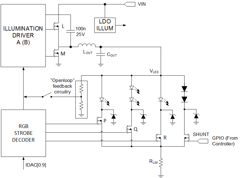
DLPA4000 DLPA4000_Illum_Control.gifFigure 4. Illumination Control Loop

These blocks comprise the illumination control loop.

  • Programmable gain block
  • LDO illum, analog supply voltage for internal illumination blocks
  • Illumination driver A, primary driver for the external FETs
  • RGB strobe decoder, driver for external switches to control the on-off rhythm of the LEDs and measures the LED current