DLPS132 May   2018 DLPA4000

PRODUCTION DATA.  

  1. Features
  2. Applications
  3. Description
    1.     Device Images
      1.      System Block Diagram
  4. Revision History
  5. Pin Configuration and Functions
    1.     Pin Functions
  6. Specifications
    1. 6.1 Absolute Maximum Ratings
    2. 6.2 ESD Ratings
    3. 6.3 Recommended Operating Conditions
    4. 6.4 Thermal Information
    5. 6.5 Electrical Characteristics
    6. 6.6 SPI Timing Parameters
  7. Detailed Description
    1. 7.1 Overview
    2. 7.2 Functional Block Description
    3. 7.3 Feature Description
      1. 7.3.1 Supply and Monitoring
        1. 7.3.1.1 Supply
        2. 7.3.1.2 Monitoring
          1. 7.3.1.2.1 Block Faults
          2. 7.3.1.2.2 Low Battery and UVLO
          3. 7.3.1.2.3 Thermal Protection
      2. 7.3.2 Illumination
        1. 7.3.2.1 Programmable Gain Block
        2. 7.3.2.2 LDO Illumination
        3. 7.3.2.3 Illumination Driver A
        4. 7.3.2.4 External MOSFETs
          1. 7.3.2.4.1 Gate series resistor (RG)
          2. 7.3.2.4.2 Gate series diode (DG)
          3. 7.3.2.4.3 Gate parallel capacitance (CG)
        5. 7.3.2.5 RGB Strobe Decoder
          1. 7.3.2.5.1 Break Before Make (BBM)
          2. 7.3.2.5.2 Openloop Voltage
          3. 7.3.2.5.3 Transient Current Limit
        6. 7.3.2.6 Illumination Monitoring
          1. 7.3.2.6.1 Power Good
          2. 7.3.2.6.2 RatioMetric Overvoltage Protection
      3. 7.3.3 External Power MOSFET Selection
        1. 7.3.3.1 Threshold Voltage
        2. 7.3.3.2 Gate Charge and Gate Timing
        3. 7.3.3.3 On-resistance RDS(on)
      4. 7.3.4 DMD Supplies
        1. 7.3.4.1 LDO DMD
        2. 7.3.4.2 DMD HV Regulator
        3. 7.3.4.3 DMD/DLPC Buck Converters
        4. 7.3.4.4 DMD Monitoring
          1. 7.3.4.4.1 Power Good
          2. 7.3.4.4.2 Overvoltage Fault
      5. 7.3.5 Buck Converters
        1. 7.3.5.1 LDO Bucks
        2. 7.3.5.2 General Purpose Buck Converters
        3. 7.3.5.3 Buck Converter Monitoring
          1. 7.3.5.3.1 Power Good
          2. 7.3.5.3.2 Overvoltage Fault
      6. 7.3.6 Auxiliary LDOs
      7. 7.3.7 Measurement System
    4. 7.4 Device Functional Modes
    5. 7.5 Programming
      1. 7.5.1 SPI
      2. 7.5.2 Interrupt
      3. 7.5.3 Fast-Shutdown in Case of Fault
      4. 7.5.4 Protected Registers
      5. 7.5.5 Writing to EEPROM
    6. 7.6 Register Maps
  8. Application and Implementation
    1. 8.1 Application Information
    2. 8.2 Typical Application
      1. 8.2.1 Design Requirements
      2. 8.2.2 Detailed Design Procedure
        1. 8.2.2.1 Component Selection for General-Purpose Buck Converters
    3. 8.3 System Example With DLPA4000 Internal Block Diagram
  9. Power Supply Recommendations
    1. 9.1 Power-Up and Power-Down Timing
  10. 10Layout
    1. 10.1 Layout Guidelines
      1. 10.1.1 LED Driver
        1. 10.1.1.1 PowerBlock Gate Control Isolation
        2. 10.1.1.2 VIN to PowerBlocks
        3. 10.1.1.3 Return Current from LEDs and RSense
        4. 10.1.1.4 RC Snubber
        5. 10.1.1.5 Capacitor Choice
      2. 10.1.2 General Purpose Buck 2
      3. 10.1.3 SPI Connections
      4. 10.1.4 RLIM Routing
      5. 10.1.5 LED Connection
    2. 10.2 Layout Example
    3. 10.3 Thermal Considerations
  11. 11Device and Documentation Support
    1. 11.1 Device Support
      1. 11.1.1 Device Nomenclature
    2. 11.2 Receiving Notification of Documentation Updates
    3. 11.3 Community Resources
    4. 11.4 Trademarks
    5. 11.5 Electrostatic Discharge Caution
    6. 11.6 Glossary
  12. 12Mechanical, Packaging, and Orderable Information
    1. 12.1 Package Option Addendum
      1. 12.1.1 Packaging Information

Package Options

Mechanical Data (Package|Pins)
Thermal pad, mechanical data (Package|Pins)
Orderable Information

Transient Current Limit

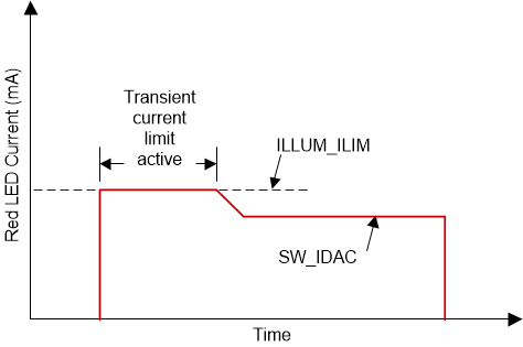
Typically the forward voltages of the green diodes and the blue diodes are equivalent to each other (between 3 V and 5 V). However the forward voltage of the red diode is significantly lower (2 V to 4 V). This difference can lead to a current spike in the RED diode when the strobe controller switches from green or blue to red. The spike occurs because the LED voltage (VLED) is initially higher than required to drive the red diode. DLPA4000 limits the transient current for each switch in the LEDs during the transition. Use register 0x02 (ILLUM_ILIM) to control the transient current limit. A typical application requires this limit for only for the RED diode. Set the value for ILLUM_ILIM to at least 20% higher than the DC regulation current. Use the three bits of register 0x02 (ILLUM_SW_ILIM_EN) to select which switch controls the transient current limiting feature. Figure 10 and Figure 11 show the effect of the transient current limit on the LED current.

For high-side pump applications, where there are two series stacked LEDs for green, sequence precautions are needed to avoid damaging the LEDS. Always transition from high-side pump green to blue, avoid following the green with red.
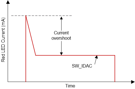
DLPA4000 transient_current_limit1_dlps132.gifFigure 10. LED Current Without Transient Current Limit
DLPA4000 transient_current_limit2_dlps132.gifFigure 11. LED Current With Transient Current Limit