DLPS096B November 2017 – May 2022 DLPC120-Q1
PRODUCTION DATA
- 1 Features
- 2 Applications
- 3 Description
- 4 Revision History
- 5 Pin Configuration and Functions
-
6 Specifications
- 6.1 Absolute Maximum Ratings
- 6.2 ESD Ratings
- 6.3 Recommended Operating Conditions
- 6.4 Thermal Information
- 6.5 Electrical Characteristics
- 6.6 Electrical Characteristics for I/O
- 6.7 Power Supply and Reset Timing Requirements
- 6.8 Reference Clock PLL Timing Requirements
- 6.9 Parallel Interface General Timing Requirements
- 6.10 Parallel Interface Frame Timing Requirements
- 6.11 Flash Memory Interface Timing Requirements
- 6.12 DMD Interface Timing Requirements
- 6.13 JTAG Interface Timing Requirements
- 6.14 I2C Interface Timing Requirements
- 7 Parameter Measurement Information
- 8 Detailed Description
- 9 Application and Implementation
- 10Power Supply Recommendations
- 11Layout
- 12Device and Documentation Support
- 13Mechanical, Packaging, and Orderable Information
Package Options
Refer to the PDF data sheet for device specific package drawings
Mechanical Data (Package|Pins)
- ZXS|216
Thermal pad, mechanical data (Package|Pins)
Orderable Information
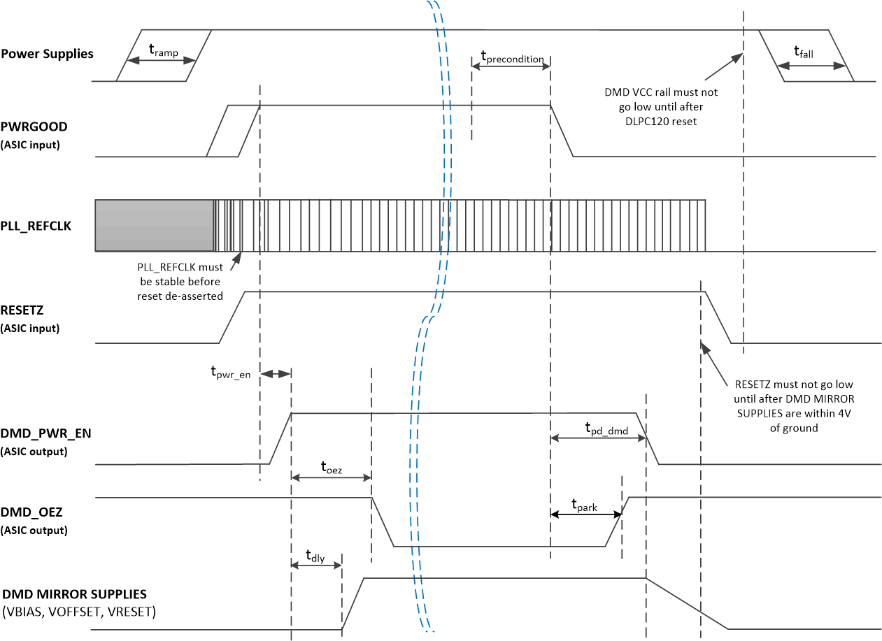
6.7 Power Supply and Reset Timing Requirements
| MIN | MAX | UNIT | |||
|---|---|---|---|---|---|
| tramp | Time for all DLPC120-Q1 power rails to be applied | Power supplies can be applied in any order if they occur within this maximum timing. Otherwise, refer to Note (1). | 10 | ms | |
| tpwr_en | RESETZ rising edge (or PWRGOOD rising edge—whichever comes second) to DMD_PWR_EN rising edge | PWRGOOD shall be controlled by LED_R_PWM / PWRGOOD_CNTRL signal, which is an output of the DLPC120-Q1 and will automatically be asserted after the device releases from reset. | 150 | µs | |
| tdly | External delay between DMD_PWR_EN and DMD mirror supply voltages | This delay is not required for supported devices. | ms | ||
| toez | DMD_PWR_EN rising edge to falling edge of DMD_OEZ | 5 | ms | ||
| tprecondition | DMD preconditioning timeI | It is required that the DMD executes a Pre-Conditioning Sequence prior to parking. The final action of this sequence is the de-assertion of the LED_R_PWM / PWRGOOD_CNTRL signal, which shall drive the PWRGOOD signal low. See the DLPC120-Q1 Programmer's Guide for instructions on how to execute the Pre-Conditioning Sequence. | 800 | µs | |
| tpark | DMD park time (approximate) | 200 | 200 | µs | |
| tpd_dmd | PWRGOOD low to falling edge of DMD_PWR_EN | 500 | µs | ||
| tfall | Time for DLPC120-Q1 power supplies to be removed | Power supplies can be removed in any order if they occur within this maximum timing. Otherwise, they shall be removed in the reverse order they were applied, per the tramp specification and Note (1). | 10 | ms | |
(1) If the DLPC120-Q1 supplies cannot be applied according to this timing specification, then they must be applied in the following order, spanning no longer than 100 ms (shall be removed in the reverse order for power down):
- Apply VCCIO_2 (3.3 V)
- Apply VCCIO_0, VCCIO_1 (1.8 V) DDR Memory and DMD, in any order
- Apply VDD (1.2 V) DLPC120-Q1 core supply voltage
 Figure 6-1 Power Supply and RESETZ Timing