DLPS014F April 2010 – May 2018 DLPC200
PRODUCTION DATA.
- 1 Features
- 2 Applications
- 3 Description
- 4 Revision History
- 5 Pin Configuration and Functions
-
6 Specifications
- 6.1 Absolute Maximum Ratings
- 6.2 Handling Ratings
- 6.3 Recommended Operating Conditions
- 6.4 Thermal Information
- 6.5 I/O Electrical Characteristics
- 6.6 Video Input Pixel Interface Timing Requirements
- 6.7 I2C Interface Timing Requirements
- 6.8 USB Read Interface Timing Requirements
- 6.9 USB Write Interface Timing Requirements
- 6.10 SPI Slave Interface Timing Requirements
- 6.11 Parallel Flash Interface Timing Requirements
- 6.12 Serial Flash Interface Timing Requirements
- 6.13 Static RAM Interface Timing Requirements
- 6.14 DMD Interface Timing Requirements
- 6.15 DLPA200 Interface Timing Requirements
- 6.16 DDR2 SDR Memory Interface Timing Requirements
- 6.17 Video Input Pixel Interface – Image Sync and Blanking Requirements
- 7 Detailed Description
-
8 Application and Implementation
- 8.1 Application Information
- 8.2
Typical Application
- 8.2.1 Design Requirements
- 8.2.2
Detailed Design Procedure
- 8.2.2.1
DLPC200 System Interfaces
- 8.2.2.1.1 DLPC200 Master, I2C Interface for EDID Programming
- 8.2.2.1.2 USB Interface
- 8.2.2.1.3 Bus Protocol
- 8.2.2.1.4 SPI Slave Interface
- 8.2.2.1.5 Parallel Flash Memory Interface
- 8.2.2.1.6 Serial Flash Memory Interface
- 8.2.2.1.7 SRAM Interface
- 8.2.2.1.8 DDR2 SDR Memory Interface
- 8.2.2.1.9 Projector Image and Control Port Signals
- 8.2.2.1.10 SDRAM Memory
- 8.2.2.1
DLPC200 System Interfaces
- 8.2.3 Application Curve
- 9 Power Supply Recommendations
- 10Layout
- 11Device and Documentation Support
- 12Mechanical, Packaging, and Orderable Information
Package Options
Mechanical Data (Package|Pins)
- ZEW|780
Thermal pad, mechanical data (Package|Pins)
Orderable Information
6.12 Serial Flash Interface Timing Requirements
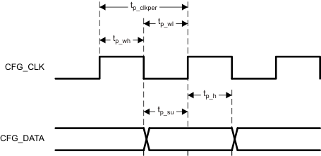
The DLPC200 controller flash memory interface consists of a SPI flash serial interface at 33.3 MHz (nominal).| PARAMETER | MIN | MAX | UNIT | |
|---|---|---|---|---|
| ƒclock | Clock frequency, CFG_CLK | dc | 33 | MHz |
| tp_clkper | Clock period, CFG_CLK | 30.03 | ns | |
| tp_wh | Pulse duration low, CFG_CLK | 6 | ns | |
| tp_wl | Pulse duration high, CFG_CLK | 6 | ns | |
| tp_su | Setup time – CFG_ASDI/CFG_ASDO valid before CFG_CLK rising edge | 2 | ns | |
| tp_h | Hold time – CFG_ASDI/CFG_ASDO valid after CFG_CLK rising edge | 5 | ns | |
