DLPS054I December 2015 – August 2024 DLPC230-Q1 , DLPC231-Q1
PRODUCTION DATA
- 1
- 1 Features
- 2 Applications
- 3 Description
- 4 Pin Configuration and Functions
-
5 Specifications
- 5.1 Absolute Maximum Ratings
- 5.2 ESD Ratings
- 5.3 Recommended Operating Conditions
- 5.4 Thermal Information
- 5.5 Electrical Characteristics
- 5.6 Electrical Characteristics for Fixed Voltage I/O
- 5.7 DMD High-Speed SubLVDS Electrical Characteristics
- 5.8 DMD Low-Speed SubLVDS Electrical Characteristics
- 5.9 OpenLDI LVDS Electrical Characteristics
- 5.10 Power Dissipation Characterisics
- 5.11 System Oscillators Timing Requirements
- 5.12 Power Supply and Reset Timing Requirements
- 5.13 Parallel Interface General Timing Requirements
- 5.14 OpenLDI Interface General Timing Requirements
- 5.15 Parallel/OpenLDI Interface Frame Timing Requirements
- 5.16 Host/Diagnostic Port SPI Interface Timing Requirements
- 5.17 Host/Diagnostic Port I2C Interface Timing Requirements
- 5.18 Flash Interface Timing Requirements
- 5.19 TPS99000-Q1 SPI Interface Timing Requirements
- 5.20 TPS99000-Q1 AD3 Interface Timing Requirements
- 5.21 DLPC23x-Q1 I2C Port Interface Timing Requirements
- 5.22 Chipset Component Usage Specification
- 6 Parameter Measurement Information
-
7 Detailed Description
- 7.1 Overview
- 7.2 Functional Block Diagram
- 7.3
Feature Description
- 7.3.1 Parallel Interface
- 7.3.2 OpenLDI Interface
- 7.3.3 DMD (SubLVDS) Interface
- 7.3.4 Serial Flash Interface
- 7.3.5 Serial Flash Programming
- 7.3.6 Host Command and Diagnostic Processor Interfaces
- 7.3.7 GPIO Supported Functionality
- 7.3.8 Built-In Self Test (BIST)
- 7.3.9 EEPROMs
- 7.3.10 Temperature Sensor
- 7.3.11 Debug Support
- 7.4 Device Functional Modes
-
8 Application and Implementation
- 8.1 Application Information
- 8.2 Typical Application
- 8.3 Power Supply Recommendations
- 8.4
Layout
- 8.4.1
Layout Guidelines
- 8.4.1.1 PCB Layout Guidelines for Internal ASIC PLL Power
- 8.4.1.2 DLPC23x-Q1 Reference Clock
- 8.4.1.3 DMD Interface Layout Considerations
- 8.4.1.4 General PCB Recommendations
- 8.4.1.5 General Handling Guidelines for Unused CMOS-Type Pins
- 8.4.1.6 Maximum Pin-to-Pin, PCB Interconnects Etch Lengths
- 8.4.1.7 Number of Layer Changes
- 8.4.1.8 Stubs
- 8.4.1.9 Terminations
- 8.4.1.10 Routing Vias
- 8.4.1.11 Layout Examples
- 8.4.2 Thermal Considerations
- 8.4.1
Layout Guidelines
- 9 Device and Documentation Support
- 10Revision History
- 11Mechanical, Packaging, and Orderable Information
Package Options
Mechanical Data (Package|Pins)
- ZDQ|324
Thermal pad, mechanical data (Package|Pins)
Orderable Information
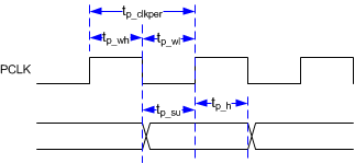
5.13 Parallel Interface General Timing Requirements
| MIN | MAX | UNIT | |||
|---|---|---|---|---|---|
| ƒclock | Clock frequency, PCLK | 12.0 | 110.0 | MHz | |
| tp_clkper | Clock period, PCLK | 50% reference points | 9.091 | 83.33 | ns |
| tp_wh | Pulse duration low, PCLK | 50% reference points | 2.286 | ns | |
| tp_wl | Pulse duration high, PCLK | 50% reference points | 2.286 | ns | |
| tp_su | Setup time – HSYNC, DATEN, PDATA(23:0) valid before the active edge of PCLK | 50% reference points | 0.8 | ns | |
| tp_h | Hold time – HSYNC, DATEN, PDATA(23:0) valid after the active edge of PCLK | 50% reference points | 0.8 | ns | |
| tt_clk | Transition time – PCLK | 20% to 80% reference points | 6 | ns | |
| tt | Transition time – all other signals on this port | 20% to 80% reference points | 6 | ns | |
| ƒspread | Supported Spread Spectrum range | Percent of ƒclock rate | –1% | +1%(1) | |
| ƒmod | Supported Spread Spectrum Modulation Frequency(1)(2) | 25 | 65(3) | kHz | |
| tp_clkjit | Clock jitter, PCLK | tp_clkper – 5.414 | ps | ||
(1) This value is limited by the maximum clock frequency for ƒclock (that is, if ƒclock = max clock freq, then ƒspread max = 0%).
(2) Modulation Waveforms supported: Sine and Triangle.
(3) Spread spectrum modulation tested at a maximum of 35 kHz. Simulated up to 65 kHz.
 Figure 5-3 Parallel Interface General Timing