DLPS201E August 2020 – August 2024 DLPC230S-Q1 , DLPC231S-Q1
PRODUCTION DATA
- 1
- 1 Features
- 2 Applications
- 3 Description
- 4 Pin Configuration and Functions
-
5 Specifications
- 5.1 Absolute Maximum Ratings
- 5.2 ESD Ratings
- 5.3 Recommended Operating Conditions
- 5.4 Thermal Information
- 5.5 Electrical Characteristics
- 5.6 Electrical Characteristics for Fixed Voltage I/O
- 5.7 DMD High-Speed SubLVDS Electrical Characteristics
- 5.8 DMD Low-Speed SubLVDS Electrical Characteristics
- 5.9 OpenLDI LVDS Electrical Characteristics
- 5.10 Power Dissipation Characterisics
- 5.11 System Oscillators Timing Requirements
- 5.12 Power Supply and Reset Timing Requirements
- 5.13 Parallel Interface General Timing Requirements
- 5.14 OpenLDI Interface General Timing Requirements
- 5.15 Parallel/OpenLDI Interface Frame Timing Requirements
- 5.16 Host/Diagnostic Port SPI Interface Timing Requirements
- 5.17 Host/Diagnostic Port I2C Interface Timing Requirements
- 5.18 Flash Interface Timing Requirements
- 5.19 TPS99000S-Q1 SPI Interface Timing Requirements
- 5.20 TPS99000S-Q1 AD3 Interface Timing Requirements
- 5.21 DLPC23xS-Q1 I2C Port Interface Timing Requirements
- 5.22 Chipset Component Usage Specification
- 6 Parameter Measurement Information
-
7 Detailed Description
- 7.1 Overview
- 7.2 Functional Block Diagram
- 7.3
Feature Description
- 7.3.1 Parallel Interface
- 7.3.2 OpenLDI Interface
- 7.3.3 DMD (SubLVDS) Interface
- 7.3.4 Serial Flash Interface
- 7.3.5 Serial Flash Programming
- 7.3.6 Host Command and Diagnostic Processor Interfaces
- 7.3.7 GPIO Supported Functionality
- 7.3.8 Built-In Self Test (BIST)
- 7.3.9 EEPROMs
- 7.3.10 Temperature Sensor
- 7.3.11 Debug Support
- 7.4 Device Functional Modes
-
8 Application and Implementation
- 8.1 Application Information
- 8.2 Typical Application
- 8.3 Power Supply Recommendations
- 8.4
Layout
- 8.4.1
Layout Guidelines
- 8.4.1.1 PCB Layout Guidelines for Internal ASIC PLL Power
- 8.4.1.2 DLPC23xS-Q1 Reference Clock
- 8.4.1.3 DMD Interface Layout Considerations
- 8.4.1.4 General PCB Recommendations
- 8.4.1.5 General Handling Guidelines for Unused CMOS-Type Pins
- 8.4.1.6 Maximum Pin-to-Pin, PCB Interconnects Etch Lengths
- 8.4.1.7 Number of Layer Changes
- 8.4.1.8 Stubs
- 8.4.1.9 Terminations
- 8.4.1.10 Routing Vias
- 8.4.2 Thermal Considerations
- 8.4.1
Layout Guidelines
- 9 Device and Documentation Support
- 10Revision History
- 11Mechanical, Packaging, and Orderable Information
Package Options
Refer to the PDF data sheet for device specific package drawings
Mechanical Data (Package|Pins)
- ZEK|324
Thermal pad, mechanical data (Package|Pins)
Orderable Information
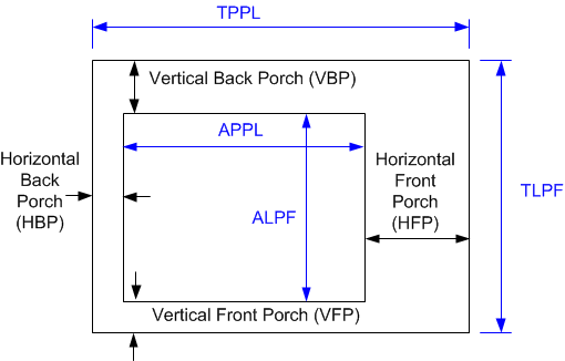
9.1.2.3 Video Timing Parameter Definitions
- Active Lines Per Frame (ALPF)Defines the number of lines in a frame containing displayable data: ALPF is a subset of the TLPF.
- Active Pixels Per Line (APPL)Defines the number of pixel clocks in a line containing displayable data: APPL is a subset of the TPPL.
- Horizontal Back Porch (HBP) BlankingNumber of blank pixel clocks after horizontal sync but before the first active pixel. Note: HBP times are reference to the leading (active) edge of the respective sync signal.
- Horizontal Front Porch (HFP) BlankingNumber of blank pixel clocks after the last active pixel but before Horizontal Sync.
- Horizontal Sync (HS)Timing reference point that defines the start of each horizontal interval (line). The absolute reference point is defined by the active edge of the HS signal. The active edge (either rising or falling edge as defined by the source) is the reference from which all horizontal blanking parameters are measured.
- Total Lines Per Frame (TLPF)Defines the vertical period (or frame time) in lines: TLPF = Total number of lines per frame (active and inactive).
- Total Pixel Per Line (TPPL)Defines the horizontal line period in pixel clocks: TPPL = Total number of pixel clocks per line (active and inactive).
- Vertical Sync (VS)Timing reference point that defines the start of the vertical interval (frame). The absolute reference point is defined by the active edge of the VS signal. The active edge (either rising or falling edge as defined by the source) is the reference from which all vertical blanking parameters are measured.
- Vertical Back Porch (VBP) BlankingNumber of blank lines after vertical sync but before the first active line.
- Vertical Front Porch (VFP) BlankingNumber of blank lines after the last active line but before vertical sync.
