DLPS201E August 2020 – August 2024 DLPC230S-Q1 , DLPC231S-Q1
PRODUCTION DATA
- 1
- 1 Features
- 2 Applications
- 3 Description
- 4 Pin Configuration and Functions
-
5 Specifications
- 5.1 Absolute Maximum Ratings
- 5.2 ESD Ratings
- 5.3 Recommended Operating Conditions
- 5.4 Thermal Information
- 5.5 Electrical Characteristics
- 5.6 Electrical Characteristics for Fixed Voltage I/O
- 5.7 DMD High-Speed SubLVDS Electrical Characteristics
- 5.8 DMD Low-Speed SubLVDS Electrical Characteristics
- 5.9 OpenLDI LVDS Electrical Characteristics
- 5.10 Power Dissipation Characterisics
- 5.11 System Oscillators Timing Requirements
- 5.12 Power Supply and Reset Timing Requirements
- 5.13 Parallel Interface General Timing Requirements
- 5.14 OpenLDI Interface General Timing Requirements
- 5.15 Parallel/OpenLDI Interface Frame Timing Requirements
- 5.16 Host/Diagnostic Port SPI Interface Timing Requirements
- 5.17 Host/Diagnostic Port I2C Interface Timing Requirements
- 5.18 Flash Interface Timing Requirements
- 5.19 TPS99000S-Q1 SPI Interface Timing Requirements
- 5.20 TPS99000S-Q1 AD3 Interface Timing Requirements
- 5.21 DLPC23xS-Q1 I2C Port Interface Timing Requirements
- 5.22 Chipset Component Usage Specification
- 6 Parameter Measurement Information
-
7 Detailed Description
- 7.1 Overview
- 7.2 Functional Block Diagram
- 7.3
Feature Description
- 7.3.1 Parallel Interface
- 7.3.2 OpenLDI Interface
- 7.3.3 DMD (SubLVDS) Interface
- 7.3.4 Serial Flash Interface
- 7.3.5 Serial Flash Programming
- 7.3.6 Host Command and Diagnostic Processor Interfaces
- 7.3.7 GPIO Supported Functionality
- 7.3.8 Built-In Self Test (BIST)
- 7.3.9 EEPROMs
- 7.3.10 Temperature Sensor
- 7.3.11 Debug Support
- 7.4 Device Functional Modes
-
8 Application and Implementation
- 8.1 Application Information
- 8.2 Typical Application
- 8.3 Power Supply Recommendations
- 8.4
Layout
- 8.4.1
Layout Guidelines
- 8.4.1.1 PCB Layout Guidelines for Internal ASIC PLL Power
- 8.4.1.2 DLPC23xS-Q1 Reference Clock
- 8.4.1.3 DMD Interface Layout Considerations
- 8.4.1.4 General PCB Recommendations
- 8.4.1.5 General Handling Guidelines for Unused CMOS-Type Pins
- 8.4.1.6 Maximum Pin-to-Pin, PCB Interconnects Etch Lengths
- 8.4.1.7 Number of Layer Changes
- 8.4.1.8 Stubs
- 8.4.1.9 Terminations
- 8.4.1.10 Routing Vias
- 8.4.2 Thermal Considerations
- 8.4.1
Layout Guidelines
- 9 Device and Documentation Support
- 10Revision History
- 11Mechanical, Packaging, and Orderable Information
Package Options
Refer to the PDF data sheet for device specific package drawings
Mechanical Data (Package|Pins)
- ZEK|324
Thermal pad, mechanical data (Package|Pins)
Orderable Information
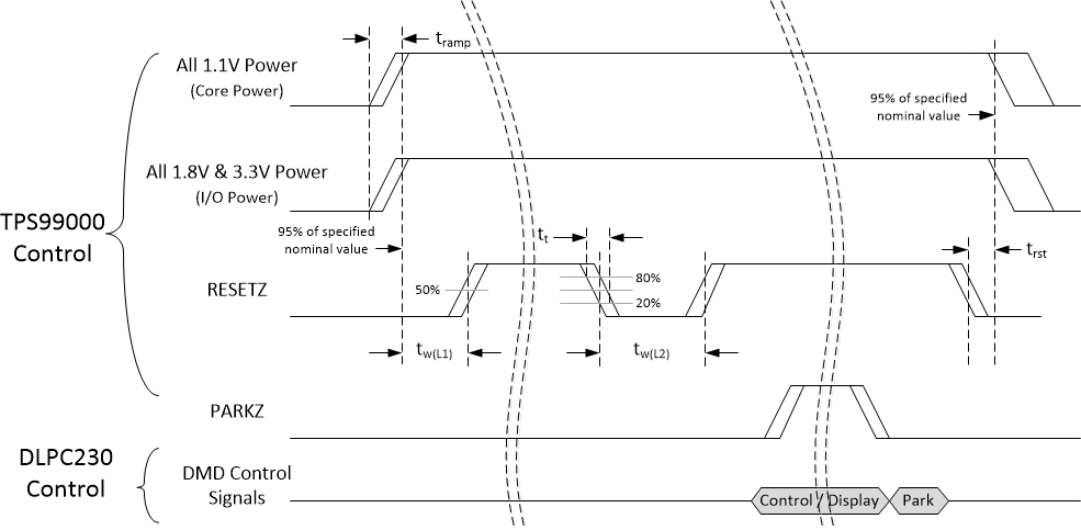
5.12 Power Supply and Reset Timing Requirements
| MIN | MAX | UNIT | |||
|---|---|---|---|---|---|
| TPS99000S-Q1 REQUIREMENTS(1) | |||||
| tramp | Power supply ramp time(2) | Power supply ramp to minimum recommended operating voltage | 0.5 | 10 | ms |
| tps_aln | 1.1V Power Supply Alignment(3) | Leading edge for application or removal of power. Each 1.1V power supply to the DLPC23xS-Q1 must be applied simultaneously within this time. | 10 | µs | |
| trst | RESETZ low to Power Supply disable(4) | Leading edge for removal of power | 1.0 | µs | |
| tw(L1) | Pulse duration, active low, RESETZ(4) | 95% power to 50% RESETZ reference point At initial application of power |
5.0 | ms | |
| tw(L2) | Pulse duration, active low, RESETZ | 50% to 50% reference points (RESETZ) Subsequent resets after initial application of power |
1.0 | µs | |
| tt | Transition time, RESETZ, tt = tƒ and tr | 20% to 80% reference points (signal) | 6 | µs | |
(1) The TPS99000S-Q1
controls power supply timing for the DLPC23xS-Q1. Refer to the TPS99000S-Q1 System Management and Illumination
Controller Data Sheet for additional system power timing
requirements.
(2) Power supplies do not need to ramp simultaneously, but each
supply must reach its minimum voltage within the maximum ramp time
specified.
(3) The DLPC23xS-Q1 does not
require specific sequencing or alignment of 1.8V and 3.3V supplies. However,
the TPS99000S-Q1 enforces
sequencing of the 1.1V, 1.8V, and 3.3V voltage rails. The following describes
DLPC23xS-Q1 behavior when the voltage rails
are not brought up simultaneously:
- VCCK (1.1V core) Power = On, I/O Power = Off, RESETZ = '0': While this condition exists, additional leakage current can be drawn, and all outputs are unknown (likely to be a weak "low").
- VCCK (1.1V core) Power = Off, I/O Power = On, RESETZ = '0': While this condition exists all outputs are tristated.
(4) RESETZ must be held low if any supply (Core or I/O) is less
than its minimum specified on value. For more information on RESETZ, see Section 4.
 Figure 5-2 Power
Supply and RESETZ Timing