DLPS231B October 2021 – October 2024 DLPC3421
PRODUCTION DATA
- 1
- 1 Features
- 2 Applications
- 3 Description
- 4 Pin Configuration and Functions
-
5 Specifications
- 5.1 Absolute Maximum Ratings
- 5.2 ESD Ratings
- 5.3 Recommended Operating Conditions
- 5.4 Thermal Information
- 5.5 Power Electrical Characteristics
- 5.6 Pin Electrical Characteristics
- 5.7 Internal Pullup and Pulldown Electrical Characteristics
- 5.8 DMD Sub-LVDS Interface Electrical Characteristics
- 5.9 DMD Low-Speed Interface Electrical Characteristics
- 5.10 System Oscillator Timing Requirements
- 5.11 Power Supply and Reset Timing Requirements
- 5.12 Parallel Interface Video Frame Timing Requirements
- 5.13 Parallel Interface General Timing Requirements
- 5.14 DSI Host Timing Requirements
- 5.15 Flash Interface Timing Requirements
- 5.16 Other Timing Requirements
- 5.17 DMD Sub-LVDS Interface Switching Characteristics
- 5.18 DMD Parking Switching Characteristics
- 5.19 Chipset Component Usage Specification
-
6 Detailed Description
- 6.1 Overview
- 6.2 Functional Block Diagram
- 6.3 Feature Description
- 6.4 Device Functional Modes
- 6.5 Programming
- 6.6 Features and System Configuration
- 7 Application and Implementation
- 8 Power Supply Recommendations
- 9 Layout
- 10Device and Documentation Support
- 11Revision History
- 12Mechanical, Packaging, and Orderable Information
- 13Package Option Addendum
Package Options
Mechanical Data (Package|Pins)
- ZVB|176
Thermal pad, mechanical data (Package|Pins)
9.1.1 PLL Power Layout
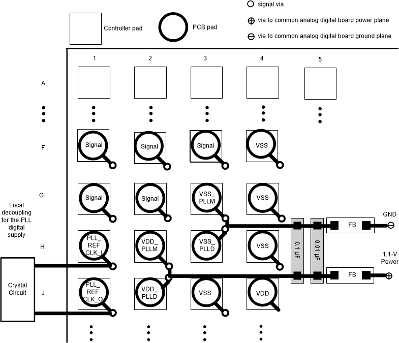
Follow these recommended guidelines to achieve acceptable controller performance for the internal PLL. The DLPC34xx controller contains two internal PLLs which have dedicated analog supplies (VDD_PLLM, VSS_PLLM, VDD_PLLD, and VSS_PLLD). At a minimum, isolate the VDD_PLLx power and VSS_PLLx ground pins using a simple passive filter consisting of two series ferrite beads and two shunt capacitors (to widen the spectrum of noise absorption). It is recommended that one capacitor be 0.1µF and one be 0.01µF. Place all four components as close to the controller as possible. It is especially important to keep the leads of the high frequency capacitors as short as possible. Connect both capacitors from VDD_PLLM to VSS_PLLM and VDD_PLLD to VSS_PLLD on the controller side of the ferrite beads.
Select ferrite beads with these characteristics:
- DC resistance less than 0.40Ω
- Impedance at 10MHz equal to or greater than 180Ω
- Impedance at 100MHz equal to or greater than 600Ω
The PCB layout is critical to PLL performance. It is vital that the quiet ground and power are treated like analog signals. Therefore, VDD_PLLM and VDD_PLLD must be a single trace from the DLPC34xx controller to both capacitors and then through the series ferrites to the power source. Make the power and ground traces as short as possible, parallel to each other, and as close as possible to each other.
 Figure 9-1 PLL
Filter Layout