DLPS231B October 2021 – October 2024 DLPC3421
PRODUCTION DATA
- 1
- 1 Features
- 2 Applications
- 3 Description
- 4 Pin Configuration and Functions
-
5 Specifications
- 5.1 Absolute Maximum Ratings
- 5.2 ESD Ratings
- 5.3 Recommended Operating Conditions
- 5.4 Thermal Information
- 5.5 Power Electrical Characteristics
- 5.6 Pin Electrical Characteristics
- 5.7 Internal Pullup and Pulldown Electrical Characteristics
- 5.8 DMD Sub-LVDS Interface Electrical Characteristics
- 5.9 DMD Low-Speed Interface Electrical Characteristics
- 5.10 System Oscillator Timing Requirements
- 5.11 Power Supply and Reset Timing Requirements
- 5.12 Parallel Interface Video Frame Timing Requirements
- 5.13 Parallel Interface General Timing Requirements
- 5.14 DSI Host Timing Requirements
- 5.15 Flash Interface Timing Requirements
- 5.16 Other Timing Requirements
- 5.17 DMD Sub-LVDS Interface Switching Characteristics
- 5.18 DMD Parking Switching Characteristics
- 5.19 Chipset Component Usage Specification
-
6 Detailed Description
- 6.1 Overview
- 6.2 Functional Block Diagram
- 6.3 Feature Description
- 6.4 Device Functional Modes
- 6.5 Programming
- 6.6 Features and System Configuration
- 7 Application and Implementation
- 8 Power Supply Recommendations
- 9 Layout
- 10Device and Documentation Support
- 11Revision History
- 12Mechanical, Packaging, and Orderable Information
- 13Package Option Addendum
Package Options
Mechanical Data (Package|Pins)
- ZVB|176
Thermal pad, mechanical data (Package|Pins)
5.12 Parallel Interface Video Frame Timing Requirements
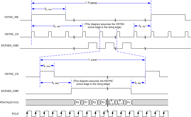
See Video Timing Parameter Definitions for additional information
| MIN | MAX | UNIT | |||
|---|---|---|---|---|---|
| tp_vsw | Pulse duration – default VSYNC_WE high | 50% reference points | 1 | lines | |
| tp_vbp | Vertical back porch (VBP) – time from the active edge of VSYNC_WE to the active edge of HSYNC_CS for the first active line(1) | 50% reference points | 2 | lines | |
| tp_vfp | Vertical front porch (VFP) – time from the active edge of the HSYNC_CS following the last active line in a frame to the active edge of VSYNC_WE(1) | 50% reference points | 1 | lines | |
| tp_tvb | Total vertical blanking – the sum of VBP and VFP (tp_vbp + tp_vfp) | 50% reference points | See (1) | lines | |
| tp_hsw | Pulse duration – default HSYNC_CS high | 50% reference points | 4 | 128 | PCLKs |
| tp_hbp | Horizontal back porch (HBP) – time from the active edge of HSYNC_CS to the rising edge of DATAEN_CMD | 50% reference points | 4 | PCLKs | |
| tp_hfp | Horizontal front porch (HFP) – time from the falling edge of DATAEN_CMD to the active edge of HSYNC_CS | 50% reference points | 8 | PCLKs | |
(1) The minimum total vertical blanking is defined by the following equation:
tp_tvb(min) = 6 + [8 × Max(1, Source_ALPF / DMD_ALPF)] lines
where:
where:
- SOURCE_ALPF = Input source active lines per frame
- DMD_ALPF = Actual DMD used lines per frame supported
 Figure 5-7 Parallel Interface Video
Frame Timing