DLPS143B July   2018  – October 2020 DLPC3434

PRODUCTION DATA  

  1. Features
  2. Applications
  3. Description
  4. Revision History
  5. Pin Configuration and Functions
    1. 5.1 Test Pins and General Control
    2. 5.2 Parallel Port Input
    3. 5.3 DSI Input Data and Clock
    4. 5.4 DMD Reset and Bias Control
    5. 5.5 DMD Sub-LVDS Interface
    6. 5.6 Peripheral Interface
    7. 5.7 GPIO Peripheral Interface
    8. 5.8 Clock and PLL Support
    9. 5.9 Power and Ground
  6. Specifications
    1. 6.1  Absolute Maximum Ratings
    2. 6.2  ESD Ratings
    3. 6.3  Recommended Operating Conditions
    4. 6.4  Thermal Information
    5. 6.5  Power Electrical Characteristics
    6. 6.6  Pin Electrical Characteristics
    7. 6.7  Internal Pullup and Pulldown Electrical Characteristics
    8. 6.8  DMD Sub-LVDS Interface Electrical Characteristics
    9. 6.9  DMD Low-Speed Interface Electrical Characteristics
    10. 6.10 System Oscillator Timing Requirements
    11. 6.11 Power Supply and Reset Timing Requirements
    12. 6.12 Parallel Interface Frame Timing Requirements
    13. 6.13 Parallel Interface General Timing Requirements
    14. 6.14 Flash Interface Timing Requirements
    15. 6.15 Other Timing Requirements
    16. 6.16 DMD Sub-LVDS Interface Switching Characteristics
    17. 6.17 DMD Parking Switching Characteristics
    18. 6.18 Chipset Component Usage Specification
  7. Detailed Description
    1. 7.1 Overview
    2. 7.2 Functional Block Diagram
    3. 7.3 Feature Description
      1. 7.3.1 Input Source Requirements
        1. 7.3.1.1 Supported Resolution and Frame Rates
        2. 7.3.1.2 Parallel Interface Data Transfer Format
        3. 7.3.1.3 3D Display
      2. 7.3.2 Device Startup
      3. 7.3.3 SPI Flash
        1. 7.3.3.1 SPI Flash Interface
        2. 7.3.3.2 SPI Flash Programming
      4. 7.3.4 I2C Interface
      5. 7.3.5 Content Adaptive Illumination Control (CAIC)
      6. 7.3.6 Local Area Brightness Boost (LABB)
      7. 7.3.7 3D Glasses Operation
      8. 7.3.8 Test Point Support
      9. 7.3.9 DMD Interface
        1. 7.3.9.1 Sub-LVDS (HS) Interface
    4. 7.4 Device Functional Modes
    5. 7.5 Programming
  8. Application and Implementation
    1. 8.1 Application Information
    2. 8.2 Typical Application
      1. 8.2.1 Design Requirements
      2. 8.2.2 Detailed Design Procedure
      3. 8.2.3 Application Curve
  9. Power Supply Recommendations
    1. 9.1 PLL Design Considerations
    2. 9.2 System Power-Up and Power-Down Sequence
    3. 9.3 Power-Up Initialization Sequence
    4. 9.4 DMD Fast Park Control (PARKZ)
    5. 9.5 Hot Plug I/O Usage
  10. 10Layout
    1. 10.1 Layout Guidelines
      1. 10.1.1 PLL Power Layout
      2. 10.1.2 Reference Clock Layout
        1. 10.1.2.1 Recommended Crystal Oscillator Configuration
      3. 10.1.3 Unused Pins
      4. 10.1.4 DMD Control and Sub-LVDS Signals
      5. 10.1.5 Layer Changes
      6. 10.1.6 Stubs
      7. 10.1.7 Terminations
      8. 10.1.8 Routing Vias
      9. 10.1.9 Thermal Considerations
    2. 10.2 Layout Example
  11. 11Device and Documentation Support
    1. 11.1 Device Support
      1. 11.1.1 Third-Party Products Disclaimer
      2. 11.1.2 Device Nomenclature
        1. 11.1.2.1 Device Markings
        2. 11.1.2.2 Video Timing Parameter Definitions
    2. 11.2 Documentation Support
      1. 11.2.1 Related Documentation
    3. 11.3 Related Links
    4. 11.4 Receiving Notification of Documentation Updates
    5. 11.5 Support Resources
    6. 11.6 Trademarks
  12. 12Mechanical, Packaging, and Orderable Information
    1. 12.1 Package Option Addendum
      1. 12.1.1 Packaging Information

Package Options

Mechanical Data (Package|Pins)
Thermal pad, mechanical data (Package|Pins)

Typical Application

A common application when using DLPC3434 controller with DLP230KP (.23 HD) and DLPA2000 PMIC/LED driver is for creating a pico projector embedded in a handheld product. For example, a pico projector may be embedded in a smart phone, a tablet, a camera, or camcorder. The DLPC3434 in the pico projector embedded module typically receives images from a host processor within the product.
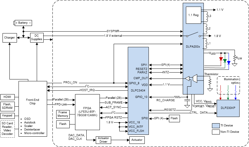
GUID-5F4363EF-31C7-4E1A-8915-BC36E991B6EB-low.gif Figure 8-1 Typical Application Diagram (using DLPA200x)
Figure 8-2 Typical Application Diagram (using DLPA3000)