DLPS143B July 2018 – October 2020 DLPC3434
PRODUCTION DATA
- 1 Features
- 2 Applications
- 3 Description
- 4 Revision History
- 5 Pin Configuration and Functions
-
6 Specifications
- 6.1 Absolute Maximum Ratings
- 6.2 ESD Ratings
- 6.3 Recommended Operating Conditions
- 6.4 Thermal Information
- 6.5 Power Electrical Characteristics
- 6.6 Pin Electrical Characteristics
- 6.7 Internal Pullup and Pulldown Electrical Characteristics
- 6.8 DMD Sub-LVDS Interface Electrical Characteristics
- 6.9 DMD Low-Speed Interface Electrical Characteristics
- 6.10 System Oscillator Timing Requirements
- 6.11 Power Supply and Reset Timing Requirements
- 6.12 Parallel Interface Frame Timing Requirements
- 6.13 Parallel Interface General Timing Requirements
- 6.14 Flash Interface Timing Requirements
- 6.15 Other Timing Requirements
- 6.16 DMD Sub-LVDS Interface Switching Characteristics
- 6.17 DMD Parking Switching Characteristics
- 6.18 Chipset Component Usage Specification
-
7 Detailed Description
- 7.1 Overview
- 7.2 Functional Block Diagram
- 7.3 Feature Description
- 7.4 Device Functional Modes
- 7.5 Programming
- 8 Application and Implementation
- 9 Power Supply Recommendations
- 10Layout
- 11Device and Documentation Support
- 12Mechanical, Packaging, and Orderable Information
Package Options
Mechanical Data (Package|Pins)
- ZVB|176
Thermal pad, mechanical data (Package|Pins)
6.13 Parallel Interface General Timing Requirements
| MIN | MAX | UNIT | |||
|---|---|---|---|---|---|
| ƒclock | PCLK frequency | 1.0 | 155.0 | MHz | |
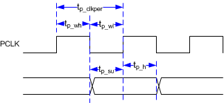
| tp_clkper | PCLK period | 50% reference points | 6.45 | 1000 | ns |
| tp_clkjit | PCLK jitter | Max ƒclock | See (1) | ||
| tp_wh | PCLK pulse duration high | 50% reference points | 2.43 | ns | |
| tp_wl | PCLK pulse duration low | 50% reference points | 2.43 | ns | |
| tp_su | Setup time – HSYNC_CS, DATAEN_CMD, PDATA(23:0) valid before the active edge of PCLK | 50% reference points | 0.9 | ns | |
| tp_h | Hold time – HSYNC_CS, DATAEN_CMD, PDATA(23:0) valid after the active edge of PCLK | 50% reference points | 0.9 | ns | |
| tt | Transition time – all signals | 20% to 80% reference points (rising signal) 80% to 20% reference points (falling signal) | 0.2 | 2.0 | ns |
| tsetup, 3DR | This is the setup time with respect to VSYNC(2) | 50% reference points | 1.0 | ms | |
| thold, 3DR | This is the hold time with respect VSYNC(3) | 50% reference points | 1.0 | ms | |
(1) Calculate clock jitter (in ns) using this formula: Jitter = [1 / ƒclock – 5.76 ns]. Setup and hold times must be met even with clock jitter.
(2) In other words, the 3DR signal must change at least 1.0 ms before VSYNC changes.
(3) In other words, the 3DR signal must not change for at least 1.0 ms after VSYNC changes.
 Figure 6-8 Parallel Interface Pixel Timing