DLPS156F January 2019 – November 2024 DLPC3436
PRODUCTION DATA
- 1
- 1 Features
- 2 Applications
- 3 Description
- 4 Pin Configuration and Functions
-
5 Specifications
- 5.1 Absolute Maximum Ratings
- 5.2 ESD Ratings
- 5.3 Recommended Operating Conditions
- 5.4 Thermal Information
- 5.5 Power Electrical Characteristics
- 5.6 Pin Electrical Characteristics
- 5.7 Internal Pullup and Pulldown Electrical Characteristics
- 5.8 DMD SubLVDS Interface Electrical Characteristics
- 5.9 DMD Low-Speed Interface Electrical Characteristics
- 5.10 System Oscillator Timing Requirements
- 5.11 Power Supply and Reset Timing Requirements
- 5.12 Parallel Interface Frame Timing Requirements
- 5.13 Parallel Interface General Timing Requirements
- 5.14 Flash Interface Timing Requirements
- 5.15 Other Timing Requirements
- 5.16 DMD SubLVDS Interface Switching Characteristics
- 5.17 DMD Parking Switching Characteristics
- 5.18 Chipset Component Usage Specification
-
6 Detailed Description
- 6.1 Overview
- 6.2 Functional Block Diagram
- 6.3 Feature Description
- 6.4 Device Functional Modes
- 6.5 Programming
- 7 Application and Implementation
- 8 Power Supply Recommendations
- 9 Layout
- 10Device and Documentation Support
- 11Revision History
- 12Mechanical, Packaging, and Orderable Information
Package Options
Mechanical Data (Package|Pins)
- ZVB|176
Thermal pad, mechanical data (Package|Pins)
Orderable Information
6.3.1.1 Input Frame Rates and 3-D Display Operation
Table 6-1 Supported Input Source Ranges
(to FPGA)(1)(2)(3)
| INTERFACE | BITS PER PIXEL (max)(4) | IMAGE TYPE | SOURCE RESOLUTION RANGE(5) | FRAME RATE RANGE | |||
|---|---|---|---|---|---|---|---|
| HORIZONTAL | VERTICAL | ||||||
| Landscape | Portrait | Landscape | Portrait | ||||
| Parallel | 24 | 2D - qHD | 960 | N/A | 540 | N/A | 50 ± 2 Hz, 60 ± 2 Hz, 100 ± 2 Hz, 120 ± 2 Hz, 200 ± 2 Hz, 240 ± 2 Hz |
| Parallel | 24 | 2D - 1080p | 1920 | N/A | 1080 | N/A | 50 ± 2 Hz, 60 ± 2 Hz |
| Parallel | 24 | 3D - qHD(6) | 960 | N/A | 540 | N/A | 100 ± 2 Hz, 120 ± 2 Hz |
(1) The application must remain within specifications for all
source interface parameters such as maximum clock rate and maximum line
rate.
(2) The maximum DMD pixel display resolution is 1920 × 1080 while system actuator is enabled.
(3) To achieve the ranges stated, the firmware must support the
source parameters. Review the firmware release notes or contact TI to determine
the latest available frame rate and input resolution support for a given
firmware image.
(4) Bits per pixel does not necessarily equal the number of data
pins used on the DLPC34xx controller. Fewer pins are used if multiple clocks are
used per pixel transfer.
(5) The DLPC34x6 only supports
landscape orientation.
(6) 3D video is formatted as frame sequential.
Table 6-2 Supported FPGA Input
Interface
| INTERFACE | IMAGE TYPE | XC7Z020-1CLG484I4493 | XC7S50-2CSGA324C4493 |
|---|---|---|---|
| Parallel | 2D - qHD | Supported | Not Supported |
| Parallel | 2D - 1080p | Supported | Not Supported |
| Parallel | 3D - qHD | Supported | Not Supported |
| FPD-Link | 2D - qHD | Supported | Supported |
| FPD-Link | 2D - 1080p | Supported | Supported |
| FPD-Link | 3D - qHD | Supported | Supported |
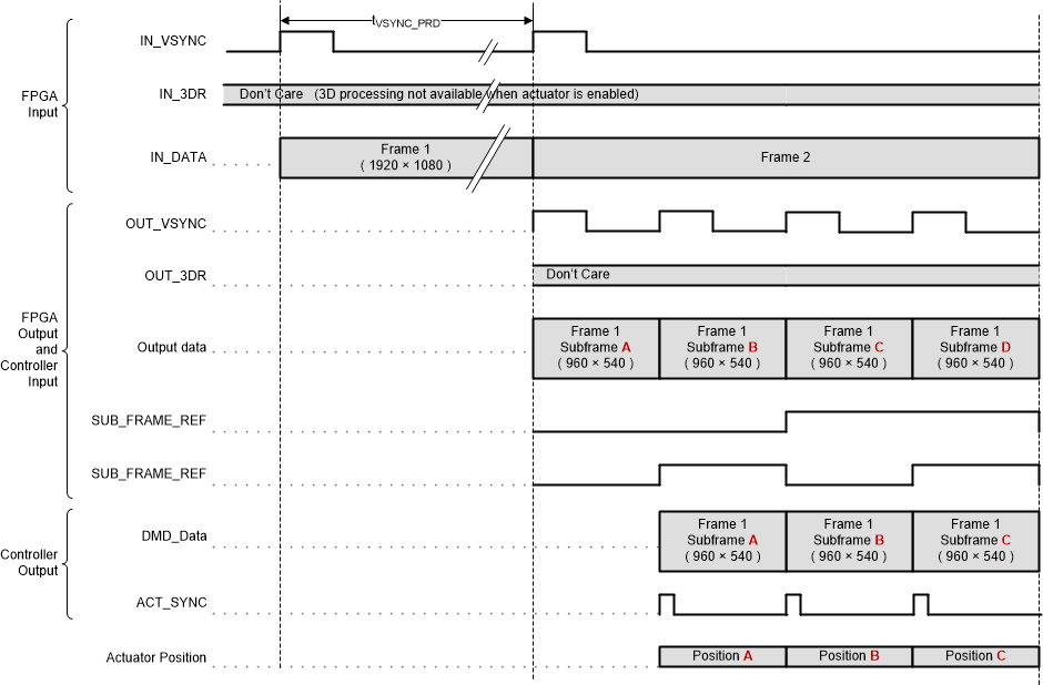
The DLPC34x6 supports both 2D and 3D sources on the parallel interface. The frame and sub-frame timing for 2D sources is shown in Figure 6-1 while the frame timing for 3D sources is shown in Figure 6-3.
 Figure 6-1 2D Actuator Frame and Signal
Timing