DLPS156F January   2019  – November 2024 DLPC3436

PRODUCTION DATA  

  1.   1
  2. Features
  3. Applications
  4. Description
  5. Pin Configuration and Functions
    1. 4.1 Test Pins and General Control
    2. 4.2 Parallel Port Input
    3. 4.3 DSI Input Data and Clock
    4. 4.4 DMD Reset and Bias Control
    5. 4.5 DMD SubLVDS Interface
    6. 4.6 Peripheral Interface
    7. 4.7 GPIO Peripheral Interface
    8. 4.8 Clock and PLL Support
    9. 4.9 Power and Ground
  6. Specifications
    1. 5.1  Absolute Maximum Ratings
    2. 5.2  ESD Ratings
    3. 5.3  Recommended Operating Conditions
    4. 5.4  Thermal Information
    5. 5.5  Power Electrical Characteristics
    6. 5.6  Pin Electrical Characteristics
    7. 5.7  Internal Pullup and Pulldown Electrical Characteristics
    8. 5.8  DMD SubLVDS Interface Electrical Characteristics
    9. 5.9  DMD Low-Speed Interface Electrical Characteristics
    10. 5.10 System Oscillator Timing Requirements
    11. 5.11 Power Supply and Reset Timing Requirements
    12. 5.12 Parallel Interface Frame Timing Requirements
    13. 5.13 Parallel Interface General Timing Requirements
    14. 5.14 Flash Interface Timing Requirements
    15. 5.15 Other Timing Requirements
    16. 5.16 DMD SubLVDS Interface Switching Characteristics
    17. 5.17 DMD Parking Switching Characteristics
    18. 5.18 Chipset Component Usage Specification
  7. Detailed Description
    1. 6.1 Overview
    2. 6.2 Functional Block Diagram
    3. 6.3 Feature Description
      1. 6.3.1 Input Source Requirements
        1. 6.3.1.1 Input Frame Rates and 3-D Display Operation
          1. 6.3.1.1.1 Parallel Interface Data Transfer Format
        2. 6.3.1.2 3D Display
      2. 6.3.2 Device Startup
      3. 6.3.3 SPI Flash
        1. 6.3.3.1 SPI Flash Interface
        2. 6.3.3.2 SPI Flash Programming
      4. 6.3.4 I2C Interface
      5. 6.3.5 Content Adaptive Illumination Control (CAIC)
      6. 6.3.6 Local Area Brightness Boost (LABB)
      7. 6.3.7 3D Glasses Operation
      8. 6.3.8 Test Point Support
      9. 6.3.9 DMD Interface
        1. 6.3.9.1 SubLVDS (HS) Interface
    4. 6.4 Device Functional Modes
    5. 6.5 Programming
  8. Application and Implementation
    1. 7.1 Application Information
    2. 7.2 Typical Application
      1. 7.2.1 Design Requirements
      2. 7.2.2 Detailed Design Procedure
      3. 7.2.3 Application Curve
  9. Power Supply Recommendations
    1. 8.1 PLL Design Considerations
    2. 8.2 System Power-Up and Power-Down Sequence
    3. 8.3 Power-Up Initialization Sequence
    4. 8.4 DMD Fast Park Control (PARKZ)
    5. 8.5 Hot Plug I/O Usage
    6. 8.6 Maximum Signal Transition Time
  10. Layout
    1. 9.1 Layout Guidelines
      1. 9.1.1 PLL Power Layout
      2. 9.1.2 Reference Clock Layout
        1. 9.1.2.1 Recommended Crystal Oscillator Configuration
      3. 9.1.3 Unused Pins
      4. 9.1.4 DMD Control and SubLVDS Signals
      5. 9.1.5 Layer Changes
      6. 9.1.6 Stubs
      7. 9.1.7 Terminations
      8. 9.1.8 Routing Vias
      9. 9.1.9 Thermal Considerations
    2. 9.2 Layout Example
  11. 10Device and Documentation Support
    1. 10.1 Device Support
      1. 10.1.1 Third-Party Products Disclaimer
      2. 10.1.2 Device Nomenclature
        1. 10.1.2.1 Device Markings DLPC343x
        2. 10.1.2.2 Device Markings DLPC342x
        3. 10.1.2.3 Video Timing Parameter Definitions
    2. 10.2 Documentation Support
      1. 10.2.1 Related Documentation
    3. 10.3 Related Links
    4. 10.4 Receiving Notification of Documentation Updates
    5. 10.5 Support Resources
    6. 10.6 Trademarks
    7. 10.7 Electrostatic Discharge Caution
    8. 10.8 Glossary
  12. 11Revision History
  13. 12Mechanical, Packaging, and Orderable Information
    1. 12.1 Package Option Addendum
      1. 12.1.1 Packaging Information

Package Options

Mechanical Data (Package|Pins)
Thermal pad, mechanical data (Package|Pins)
Orderable Information

Description

The DLPC3436 and DLPC3426 display controllers, components of the DLP230NP or DLP230NPSE .23 1080p chipset, support reliable operation of the DLP230NP/NPSE digital micromirror device (DMD). The DLPC34x6 controller provides a convenient, multifunctional interface between system electronics and the DMD, enabling a small form factor, low power, and full HD displays.

Visit the Getting Started with TI DLP® PicoTM Display Technology page to learn more about DMD technology.

The DLP230NP/NPSE .23 1080p chipset includes established resources to help the user accelerate the design cycle, which include production ready optical modules, optical modules manufactures, and design houses.

Device Compatibility
CONTROLLERDMDDESCRIPTION
DLPC3436DLP230NPHigher brightness
DLPC3426DLP230NPSELower brightness
Device Information
PART NUMBERPACKAGE(1)PACKAGE SIZE (NOM)
DLPC3436NFBGA (176)7.00mm × 7.00mm
DLPC3426NFBGA (176)7.00mm × 7.00mm
For more information, see the Mechanical, Packaging, and Orderable sections.
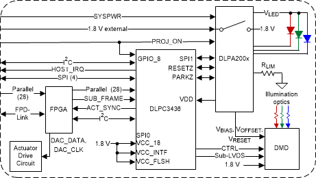
DLPC3436 Typical, Simplified SystemTypical, Simplified System