DLPS223A December 2021 – February 2023 DLPC4430
PRODUCTION DATA
- 1 Features
- 2 Applications
- 3 Description
- 4 Revision History
- 5 Pin Configuration and Functions
-
6 Specifications
- 6.1 Absolute Maximum Ratings
- 6.2 ESD Ratings
- 6.3 Recommended Operating Conditions
- 6.4 Thermal Information
- 6.5 Electrical Characteristics
- 6.6 System Oscillators Timing Requirements
- 6.7 Test and Reset Timing Requirements
- 6.8 JTAG Interface: I/O Boundary Scan Application Timing Requirements
- 6.9 Port 1 Input Pixel Timing Requirements
- 6.10 Port 3 Input Pixel Interface (via GPIO) Timing Requirements
- 6.11 DMD LVDS Interface Timing Requirements
- 6.12 Synchronous Serial Port (SSP) Interface Timing Requirements
- 6.13 Programmable Output Clocks Switching Characteristics
- 6.14 Synchronous Serial Port Interface (SSP) Switching Characteristics
- 6.15 JTAG Interface: I/O Boundary Scan Application Switching Characteristics
-
7 Detailed Description
- 7.1 Overview
- 7.2 Functional Block Diagram
- 7.3 Feature Description
- 7.4 Device Functional Modes
- 8 Application and Implementation
- 9 Power Supply Recommendations
- 10Layout
- 11Device and Documentation Support
- 12Mechanical, Packaging, and Orderable Information
Package Options
Mechanical Data (Package|Pins)
- ZPC|516
Thermal pad, mechanical data (Package|Pins)
Orderable Information
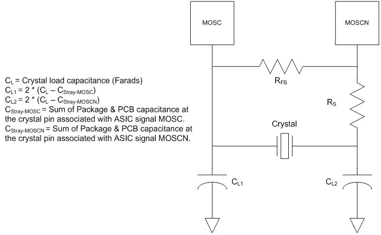
8.2.1.1 Recommended MOSC Crystal Oscillator Configuration
Table 8-1 Crystal Port Characteristics
| PARAMETER | NOMINAL | UNIT |
|---|---|---|
| MOSC TO GROUND Capacitance | 1.5 | pF |
| MOSCZ TO GROUND Capacitance | 1.5 | pF |
Table 8-2 Recommended Crystal Configuration
| PARAMETER | RECOMMENDED | UNIT |
|---|---|---|
| Crystal circuit configuration | Parallel resonant | |
| Crystal type | Fundamental (1st harmonic) | |
| Crystal nominal frequency | 20 | MHz |
| Crystal frequency temperature stability | +/– 30 | PPM |
| Overall crystal frequency tolerance (including accuracy, stability, aging, and trim sensitivity) | +/– 100 | PPM |
| Crystal Equivalent Series Resistor (ESR) | 50 max | Ω |
| Crystal load | 20 | pF |
| Crystal shunt load | 7 max | pF |
| RS drive resistor (nominal) | 100 | Ω |
| RFB feedback resistor (nominal) | 1 | MΩ |
| CL1 external crystal load capacitor (MOSC) | See (1). | pF |
| CL2 external crystal load capacitor (MOSCN) | See (1). | pF |
| PCB layout | A ground isolation ring around the crystal is recommended. |
(1) Typical drive level with the XSA020000FK1H-OCX Crystal (ESRmax = 40 Ω) = 50 µW.
 Figure 8-3 Recommended Crystal Oscillator Configuration
Typically, the external crystal oscillator stabilizes within 50 ms after stable power is applied.