DLPS168C May 2021 – November 2022 DLPC6540
PRODUCTION DATA
- 1 Features
- 2 Applications
- 3 Description
- 4 Revision History
- 5 Pin Configuration and Functions
-
6 Specifications
- 6.1 Absolute Maximum Ratings
- 6.2 ESD Ratings
- 6.3 Recommended Operating Conditions
- 6.4 Thermal Information
- 6.5 Power Electrical Characteristics
- 6.6 Pin Electrical Characteristics
- 6.7 DMD HSSI Electrical Characteristics
- 6.8 DMD Low-Speed LVDS Electrical Characteristics
- 6.9 V-by-One Interface Electrical Characteristics
- 6.10 USB Electrical Characteristics
- 6.11 System Oscillator Timing Requirements
- 6.12 Power Supply and Reset Timing Requirements
- 6.13 DMD HSSI Timing Requirements
- 6.14 DMD Low-Speed LVDS Timing Requirements
- 6.15 V-by-One Interface General Timing Requirements
- 6.16 Source Frame Timing Requirements
- 6.17 Synchronous Serial Port Interface Timing Requirements
- 6.18 Master and Slave I2C Interface Timing Requirements
- 6.19 Programmable Output Clock Timing Requirements
- 6.20 JTAG Boundary Scan Interface Timing Requirements (Debug Only)
- 6.21 JTAG ARM Multi-Ice Interface Timing Requirements (Debug Only)
- 6.22 Multi-Trace ETM Interface Timing Requirements
- 7 Detailed Description
- 8 Power Supply Recommendations
-
9 Layout
- 9.1
Layout Guidelines
- 9.1.1 General Layout Guidelines
- 9.1.2 Power Supply Layout Guidelines
- 9.1.3 Layout Guidelines for Internal Controller PLL Power
- 9.1.4 Layout Guideline for DLPC6540 Reference Clock
- 9.1.5 V-by-One Interface Layout Considerations
- 9.1.6 USB Interface Layout Considerations
- 9.1.7 DMD Interface Layout Considerations
- 9.1.8 General Handling Guidelines for Unused CMOS-Type Pins
- 9.1.9 Maximum Pin-to-Pin, PCB Interconnects Etch Lengths
- 9.2 Thermal Considerations
- 9.1
Layout Guidelines
- 10Device and Documentation Support
- 11Mechanical, Packaging, and Orderable Information
Package Options
Mechanical Data (Package|Pins)
- ZDC|676
Thermal pad, mechanical data (Package|Pins)
Orderable Information
6.15 V-by-One Interface General Timing Requirements
| PARAMETER(1) | MIN | MAX | UNIT | ||
|---|---|---|---|---|---|
| fclock | Source clock frequency | 40 (1 lane) 20 (1 lane with Pixel Repeat) (2) | 600 (8 lanes) | MHz | |
| flink-ck | Link clock frequency per lane (3) | 8 lanes 4 lanes 2 lanes 1 lane | 43 43 43 43 (21.5 with Pixel Repeat) | 75 85 85 85 | MHz |
| flink | Link transfer rate (3) | 3-Byte Mode 4-Byte Mode 5-Byte Mode | 2 2 2.15 | 2.55 3.0 3.0 | Gbps |
| tRBIT | Unit interval | 3-Byte Mode 4-Byte Mode 5-Byte Mode | 392 294 294 | 500 500 500 | ps ps ps |
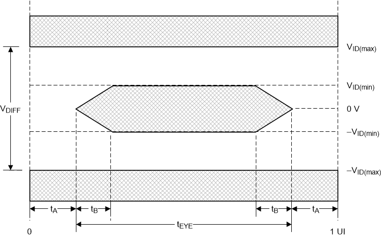
| tA | Jitter Margin | 0.25 | UI | ||
| tB | Rise / Fall Time | 0.05 | UI | ||
| tEYE | Differential Data Eye | 0.5 | UI | ||
| tskew_intra | Allowable intra-pair skew | 0.3 | UI | ||
| tskew_inter | Allowable Inter-pair Skew | 5 | UI | ||
| foskew_inter | Allowable inter-pair frequency offset | –300 | 300 | ppm | |
| Tj | Total jitter | — | 0.5 | UI | |
| Rj | Random jitter | 10^12 UI | - | 0.2 | UI |
| Dj_ISI | Deterministic jitter (ISI) | - | 0.2 | UI | |
| Sj | Sinusoidal jitter | - | 0.1 | UI | |
(1) V-by-One high-speed technology supports 1, 2,
4,
or 8 lane operation, in addition to
3-byte,
4-byte, and
5-byte
transfer
modes.
(2) Pixel repeat is a method used to support slower clock rate sources,
whereby, the source come at twice the original clock rate, with each data pixel
being repeated once, and blanking being doubled as well. This method must
operate external to DLPC6540. Once received, the DLPC6540 discards each duplicate data pixel and blanking clock.
Pixel repeat is supported only during 1- lane operation.
(3) For V-by-One high-speed technology, both link clock rate and link transfer rate limits must be met for any source.
 Figure 6-13 V-by-One Timing