DLPS271 April 2024 DLPC7530
PRODUCTION DATA
- 1
- 1 Features
- 2 Applications
- 3 Description
- 4 Pin Configuration and Functions
-
5 Specifications
- 5.1 Absolute Maximum Ratings
- 5.2 ESD Ratings
- 5.3 Recommended Operating Conditions
- 5.4 Thermal Information
- 5.5 Power Electrical Characteristics
- 5.6 Pin Electrical Characteristics
- 5.7 DMD HSSI Electrical Characteristics
- 5.8 DMD Low-Speed LVDS Electrical Characteristics
- 5.9 V-by-One Interface Electrical Characteristics
- 5.10 FPD-Link LVDS Electrical Characteristics
- 5.11 USB Electrical Characteristics
- 5.12 System Oscillator Timing Requirements
- 5.13 Power Supply and Reset Timing Requirements
- 5.14 DMD HSSI Timing Requirements
- 5.15 DMD Low-Speed LVDS Timing Requirements
- 5.16 V-by-One Interface General Timing Requirements
- 5.17 FPD-Link Interface General Timing Requirements
- 5.18 Parallel Interface General Timing Requirements
- 5.19 Source Frame Timing Requirements
- 5.20 Synchronous Serial Port Interface Timing Requirements
- 5.21 Controller and Target I2C Interface Timing Requirements
- 5.22 Programmable Output Clock Timing Requirements
- 5.23 JTAG Boundary Scan Interface Timing Requirements (Debug Only)
- 5.24 JTAG ARM Multi-Ice Interface Timing Requirements (Debug Only)
- 5.25 Multi-Trace ETM Interface Timing Requirements
- 6 Detailed Description
- 7 Application and Implementation
- 8 Power Supply Recommendations
-
9 Layout
- 9.1
Layout Guidelines
- 9.1.1 General Layout Guidelines
- 9.1.2 Power Supply Layout Guidelines
- 9.1.3 Layout Guidelines for Internal Controller PLL Power
- 9.1.4 Layout Guideline for DLPC7530 Reference Clock
- 9.1.5 V-by-One Interface Layout Considerations
- 9.1.6 FPD-Link Interface Layout Considerations
- 9.1.7 USB Interface Layout Considerations
- 9.1.8 DMD Interface Layout Considerations
- 9.1.9 General Handling Guidelines for Unused CMOS-Type Pins
- 9.1.10 Maximum Pin-to-Pin, PCB Interconnects Etch Lengths
- 9.2 Thermal Considerations
- 9.1
Layout Guidelines
- 10Device and Documentation Support
- 11Revision History
- 12Mechanical, Packaging, and Orderable Information
Package Options
Mechanical Data (Package|Pins)
- ZDC|676
Thermal pad, mechanical data (Package|Pins)
Orderable Information
5.17 FPD-Link Interface General Timing Requirements
| PARAMETER | MIN | MAX | UNIT | ||
|---|---|---|---|---|---|
| ƒclock | Clock frequency, FPDA_CLK_P/N, FPDB_CLK_P/N | 20.0 (1 port) 10 (1 port with pixel repeat)(1) |
330 (165 per port) |
MHz | |
| tclock | Clock period, FPDA_CLK_P/N, FPDB_CLK_P/N | 3.03 (6.06 per port) |
50 (1 port) 100 (1 port with pixel repeat) (1) |
ns | |
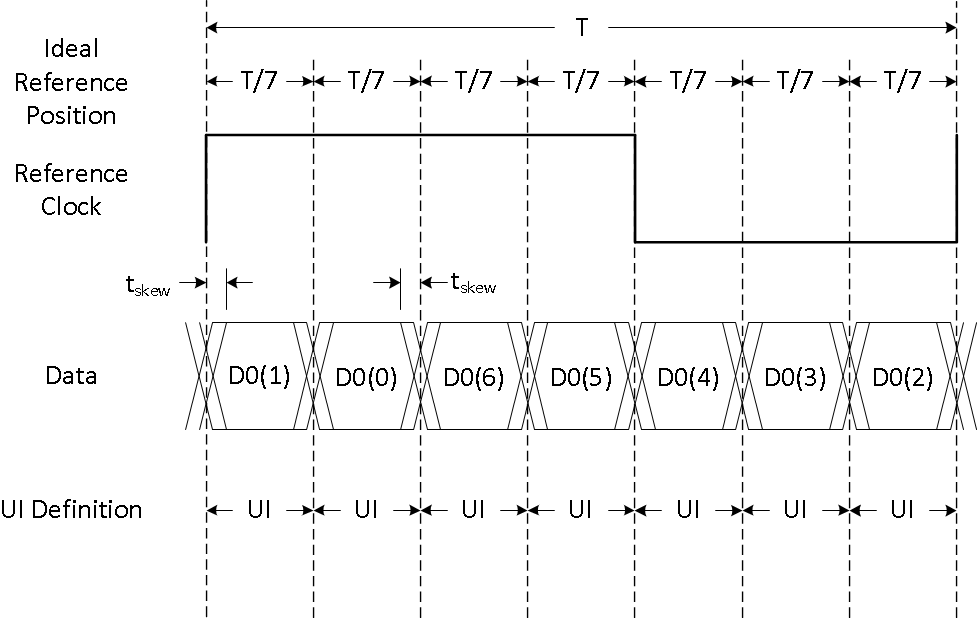
| tRBIT | Unit interval (Figure 5-14) | 0.865 (per port) | 7.143 (1 port) | ns | |
| tskew_ports | Clock to clock skew margin between ports on the same controller, and between ports on different controllers | 1 | clocks | ||
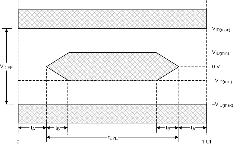
| tA | Jitter margin and skew margin between clock and data (on the same port) (Figure 5-15) | ƒclock ≤ 90 MHz | 0.25 | UI | |
| ƒclock > 90 MHz | 0.23 | UI | |||
| tB | Rise/fall time (Figure 5-15) | ƒclock ≤ 90 MHz | 333 | ps | |
| ƒclock > 90 MHz | 200 | ps | |||
| tEYE | Differential data eye (Figure 5-15) | ƒclock ≤ 90 MHz | 0.50 | UI | |
| ƒclock > 90 MHz | 0.54 | UI | |||
(1) Pixel repeat is a method used to support slower clock rate sources, whereby, the
source
comes
at twice the "original" clock rate, with each data pixel
repeated
once, and blanking
is
doubled. Both the pixel doubling and double blanking must be done external to
DLPC7530. The DLPC7530 discards each
duplicate data pixel and blanking clock. The device supports
a
pixel repeat only when using
one
port.
 Figure 5-14 FPD-Link
Data Skew
 Figure 5-15 FPD-Link
Timing