DLPS271 April 2024 DLPC7530
PRODUCTION DATA
- 1
- 1 Features
- 2 Applications
- 3 Description
- 4 Pin Configuration and Functions
-
5 Specifications
- 5.1 Absolute Maximum Ratings
- 5.2 ESD Ratings
- 5.3 Recommended Operating Conditions
- 5.4 Thermal Information
- 5.5 Power Electrical Characteristics
- 5.6 Pin Electrical Characteristics
- 5.7 DMD HSSI Electrical Characteristics
- 5.8 DMD Low-Speed LVDS Electrical Characteristics
- 5.9 V-by-One Interface Electrical Characteristics
- 5.10 FPD-Link LVDS Electrical Characteristics
- 5.11 USB Electrical Characteristics
- 5.12 System Oscillator Timing Requirements
- 5.13 Power Supply and Reset Timing Requirements
- 5.14 DMD HSSI Timing Requirements
- 5.15 DMD Low-Speed LVDS Timing Requirements
- 5.16 V-by-One Interface General Timing Requirements
- 5.17 FPD-Link Interface General Timing Requirements
- 5.18 Parallel Interface General Timing Requirements
- 5.19 Source Frame Timing Requirements
- 5.20 Synchronous Serial Port Interface Timing Requirements
- 5.21 Controller and Target I2C Interface Timing Requirements
- 5.22 Programmable Output Clock Timing Requirements
- 5.23 JTAG Boundary Scan Interface Timing Requirements (Debug Only)
- 5.24 JTAG ARM Multi-Ice Interface Timing Requirements (Debug Only)
- 5.25 Multi-Trace ETM Interface Timing Requirements
- 6 Detailed Description
- 7 Application and Implementation
- 8 Power Supply Recommendations
-
9 Layout
- 9.1
Layout Guidelines
- 9.1.1 General Layout Guidelines
- 9.1.2 Power Supply Layout Guidelines
- 9.1.3 Layout Guidelines for Internal Controller PLL Power
- 9.1.4 Layout Guideline for DLPC7530 Reference Clock
- 9.1.5 V-by-One Interface Layout Considerations
- 9.1.6 FPD-Link Interface Layout Considerations
- 9.1.7 USB Interface Layout Considerations
- 9.1.8 DMD Interface Layout Considerations
- 9.1.9 General Handling Guidelines for Unused CMOS-Type Pins
- 9.1.10 Maximum Pin-to-Pin, PCB Interconnects Etch Lengths
- 9.2 Thermal Considerations
- 9.1
Layout Guidelines
- 10Device and Documentation Support
- 11Revision History
- 12Mechanical, Packaging, and Orderable Information
Package Options
Mechanical Data (Package|Pins)
- ZDC|676
Thermal pad, mechanical data (Package|Pins)
Orderable Information
6.3.3 Parallel Interface
The DLPC7530 Controller supports a single 30-bit parallel interface which complies with standard graphics interface protocol, which includes a vertical sync signal (VSYNC), horizontal sync signal (HSYNC), data valid signal (DATEN), a 30-bit data bus (PDATA_xy), and a pixel clock (PCLK). The polarity of both syncs is programmable. Parallel Interface General Timing Requirements shows the relationship between these signals. For data sources with fewer than 10 bits/component, data must be MSB justified per component.
The input pins for FPD Ports A and B are shared by the Parallel Port. These pins can be used for FPD operation or Parallel Port operation, based on product configuration. It is not possible to switch between these two interface configurations during normal operation. Pins for FPD Port C are reserved for Parallel Port use, and can only be used when Parallel Port operation is configured
VSYNC must remain active at all times when the parallel port is in use. If VSYNC is lost, the DMD must be transitioned to a safe state. When the system detects a VSYNC loss, it switches to a test pattern or splash image as specified in flash by the Host.
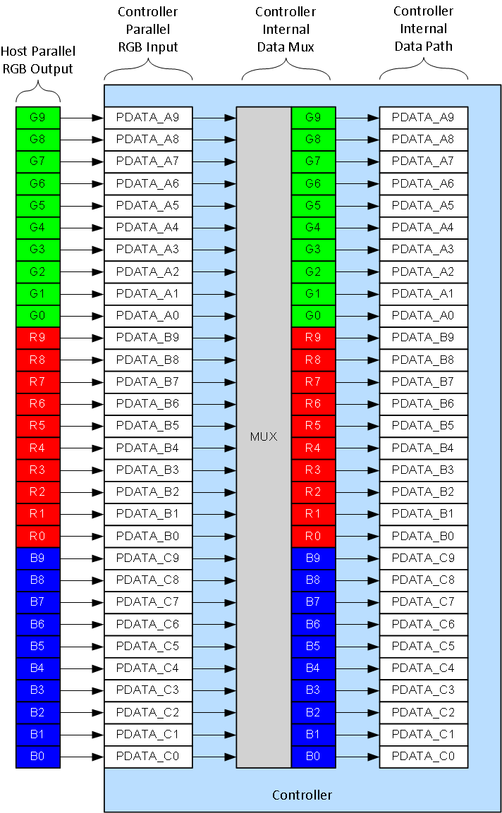
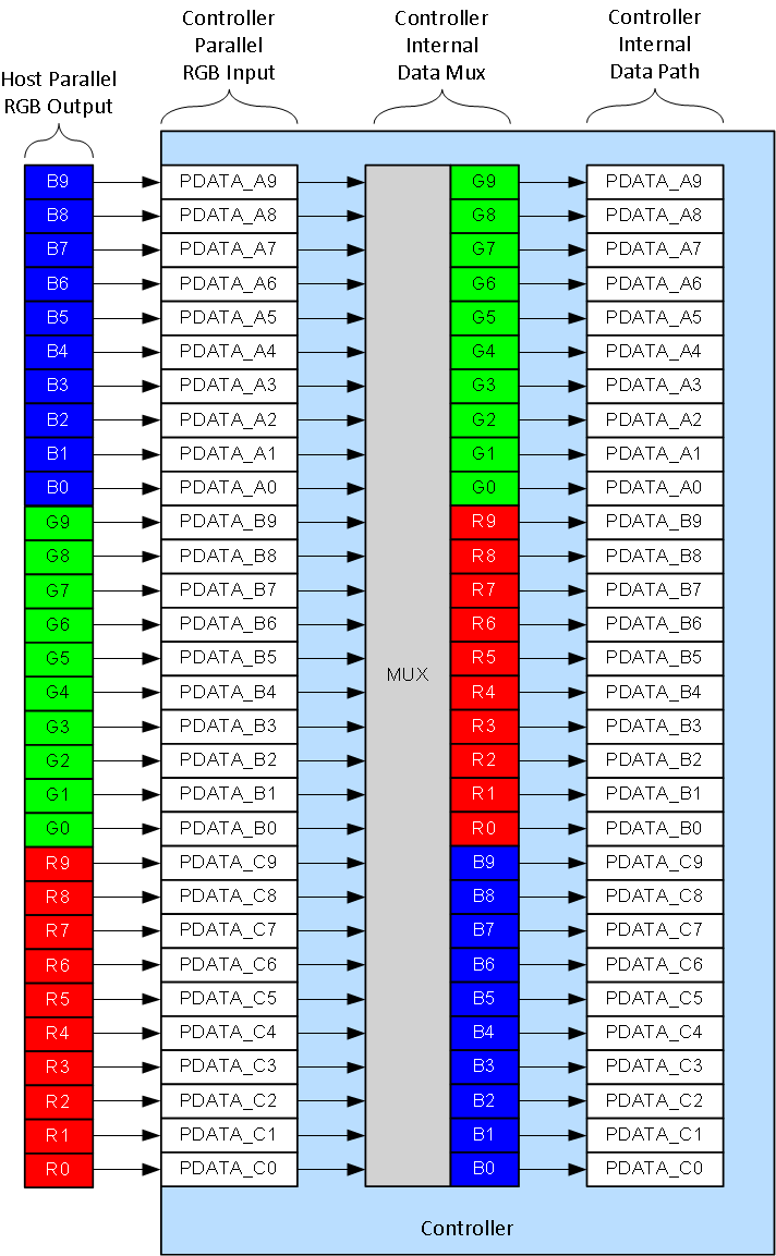
The parallel port interface supports limited inter-channel remapping (specified in flash) that can help with board layout as needed. The inter-channel remapping allows the full data bus for channel A (PDATA_Ax), B (PDATA_Bx), or C (PDATA_Cx) to be remapped to either of the other two data channels. Each input channel can only be mapped to one unique destination channel. The typical mapping is shown in Figure 6-2. An example of an alternate mapping is shown in Figure 6-3. Parallel port channel remapping is specific to parallel port operation only, and is not applicable to FPD operation.
 Figure 6-2 Standard
Parallel Port Channel Mapping
 Figure 6-3 Example
of Alternate Parallel Port Channel Mapping