DLPS271 April 2024 DLPC7530
PRODUCTION DATA
- 1
- 1 Features
- 2 Applications
- 3 Description
- 4 Pin Configuration and Functions
-
5 Specifications
- 5.1 Absolute Maximum Ratings
- 5.2 ESD Ratings
- 5.3 Recommended Operating Conditions
- 5.4 Thermal Information
- 5.5 Power Electrical Characteristics
- 5.6 Pin Electrical Characteristics
- 5.7 DMD HSSI Electrical Characteristics
- 5.8 DMD Low-Speed LVDS Electrical Characteristics
- 5.9 V-by-One Interface Electrical Characteristics
- 5.10 FPD-Link LVDS Electrical Characteristics
- 5.11 USB Electrical Characteristics
- 5.12 System Oscillator Timing Requirements
- 5.13 Power Supply and Reset Timing Requirements
- 5.14 DMD HSSI Timing Requirements
- 5.15 DMD Low-Speed LVDS Timing Requirements
- 5.16 V-by-One Interface General Timing Requirements
- 5.17 FPD-Link Interface General Timing Requirements
- 5.18 Parallel Interface General Timing Requirements
- 5.19 Source Frame Timing Requirements
- 5.20 Synchronous Serial Port Interface Timing Requirements
- 5.21 Controller and Target I2C Interface Timing Requirements
- 5.22 Programmable Output Clock Timing Requirements
- 5.23 JTAG Boundary Scan Interface Timing Requirements (Debug Only)
- 5.24 JTAG ARM Multi-Ice Interface Timing Requirements (Debug Only)
- 5.25 Multi-Trace ETM Interface Timing Requirements
- 6 Detailed Description
- 7 Application and Implementation
- 8 Power Supply Recommendations
-
9 Layout
- 9.1
Layout Guidelines
- 9.1.1 General Layout Guidelines
- 9.1.2 Power Supply Layout Guidelines
- 9.1.3 Layout Guidelines for Internal Controller PLL Power
- 9.1.4 Layout Guideline for DLPC7530 Reference Clock
- 9.1.5 V-by-One Interface Layout Considerations
- 9.1.6 FPD-Link Interface Layout Considerations
- 9.1.7 USB Interface Layout Considerations
- 9.1.8 DMD Interface Layout Considerations
- 9.1.9 General Handling Guidelines for Unused CMOS-Type Pins
- 9.1.10 Maximum Pin-to-Pin, PCB Interconnects Etch Lengths
- 9.2 Thermal Considerations
- 9.1
Layout Guidelines
- 10Device and Documentation Support
- 11Revision History
- 12Mechanical, Packaging, and Orderable Information
Package Options
Mechanical Data (Package|Pins)
- ZDC|676
Thermal pad, mechanical data (Package|Pins)
Orderable Information
9.1.3 Layout Guidelines for Internal Controller PLL Power
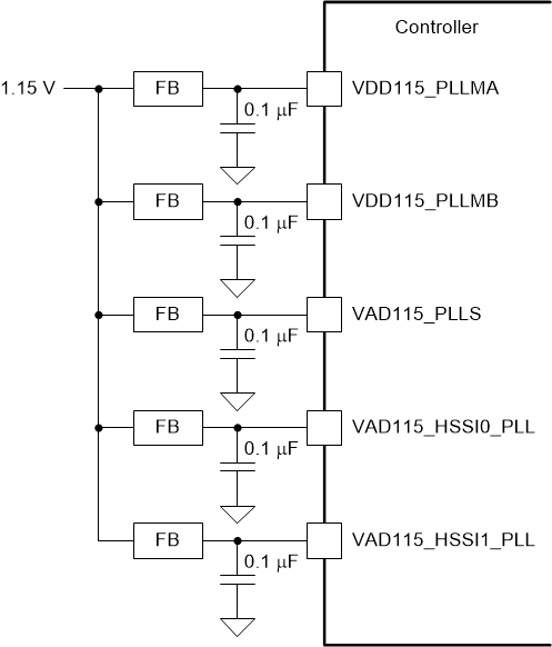
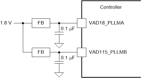
The following guidelines are recommended to achieve the desired Controller performance relative to the internal PLLs. The DLPC7530 contains multiple internal PLLs which have dedicated 1.15-V supply pins and 1.8-V supply pins which are listed below:
- VDD115_PLLMA
- VDD115_PLLMB
- VAD115_PLLS
- VAD115_HSSI0_PLL
- VAD115_HSSI1_PLL
and
- VAD18_PLLMA
- VAD18_PLLMB
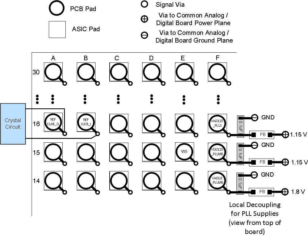
It is important that each of these 1.15-V and 1.8-V supply pins have individual high frequency filtering in the form of a ferrite bead and a 0.1-µF ceramic capacitor. Ensure that the impedance of the ferrite bead is much greater than that of the capacitor at frequencies above 10 MHz. Locate these components very close to the individual PLL power supply balls. Recommended values, topology, and layout examples are shown in Table 9-1, Figure 9-7 and Figure 9-8, and Figure 9-9 respectively.
| COMPONENT | PARAMETER | RECOMMENDED VALUE | UNIT |
|---|---|---|---|
| Shunt capacitor | Capacitance | 0.1 | µF |
| Series ferrite | Impedance at 100 MHz | > 100 | Ω |
| DC Resistance | < 0.40 | Ω |
 Figure 9-7 1.15-V
PLL Power Supply Filter Topology
 Figure 9-8 1.8-V PLL
Power Supply Filter Topology
 Figure 9-9 PLL Power Supply Filter Layout Examples
Since the PCB layout is critical to PLL performance, it is vital that the PLL power is treated like an analog signal. Additional design guidelines are as follows:
- Place all filter components as close to possible to each of the PLL supply package pins.
- Keep the leads of the high-frequency capacitors as short as possible, and as such, it is recommended that these capacitors be placed under the package on the opposite side of the board.
- Use a surface mount capacitor that is of high quality, low ESR, and monolithic.
- For each PLL power pin, a single trace (as wide as possible) must be used from the DLPC7530 to the capacitor and then through the series ferrite to the power source.