DLPS037H October 2014 – June 2024 DLPC900
PRODUCTION DATA
- 1
- 1 Features
- 2 Applications
- 3 Description
- 4 Pin Configuration and Functions
-
5 Specifications
- 5.1 Absolute Maximum Ratings
- 5.2 ESD Ratings
- 5.3 Recommended Operating Conditions
- 5.4 Thermal Information
- 5.5 Electrical Characteristics
- 5.6 System Oscillators Timing Requirements #GUID-909D0FD3-84C7-4481-924A-4FDE7EB548A1/DLPS0373944
- 5.7 Power-Up and Power-Down Timing Requirements
- 5.8 JTAG Interface: I/O Boundary Scan Application Timing Requirements
- 5.9 JTAG Interface: I/O Boundary Scan Application Switching Characteristics
- 5.10 Programmable Output Clocks Switching Characteristics
- 5.11 Port 1 and 2 Input Pixel Interface Timing Requirements
- 5.12 Two Pixels Per Clock (48-Bit Bus) Timing Requirements
- 5.13 Synchronous Serial Port (SSP) Switching Characteristics
- 5.14 DMD Interface Switching Characteristics
- 5.15 DMD LVDS Interface Switching Characteristics
- 5.16 Source Input Blanking Requirements
-
6 Detailed Description
- 6.1 Overview
- 6.2 Functional Block Diagram
- 6.3
Feature Description
- 6.3.1 DMD Configurations
- 6.3.2 Video Timing Input Blanking Specification
- 6.3.3 Board-Level Test Support
- 6.3.4 Two Controller Considerations
- 6.3.5 Memory Design Considerations
- 6.4 Device Functional Modes
-
7 Application and Implementation
- 7.1 Application Information
- 7.2
Typical Applications
- 7.2.1 Typical Two Controller Chipset
- 7.2.2 Typical Single Controller Chipset
- 8 Power Supply Recommendations
-
9 Layout
- 9.1
Layout Guidelines
- 9.1.1 General PCB Recommendations
- 9.1.2 PCB Layout Guidelines for Internal Controller PLL Power
- 9.1.3 PCB Layout Guidelines for Quality Video Performance
- 9.1.4 Recommended MOSC Crystal Oscillator Configuration
- 9.1.5 Spread Spectrum Clock Generator Support
- 9.1.6 GPIO Interface
- 9.1.7 General Handling Guidelines for Unused CMOS-Type Pins
- 9.1.8 DMD Interface Considerations
- 9.1.9 PCB Design Standards
- 9.1.10 Signal Layers
- 9.1.11 Trace Widths and Minimum Spacing
- 9.1.12 Trace Impedance and Routing Priority
- 9.1.13 Power and Ground Planes
- 9.1.14 Power Vias
- 9.1.15 Decoupling
- 9.1.16 Fiducials
- 9.2 Layout Example
- 9.3 Thermal Considerations
- 9.1
Layout Guidelines
- 10Device and Documentation Support
- 11Revision History
- 12Mechanical, Packaging, and Orderable Information
Package Options
Mechanical Data (Package|Pins)
- ZPC|516
Thermal pad, mechanical data (Package|Pins)
Orderable Information
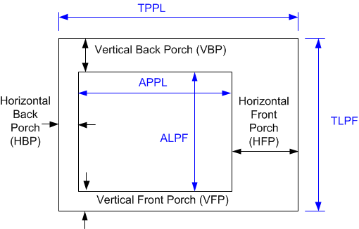
5.16 Source Input Blanking Requirements
| PORT | PARAMETER (1) | MINIMUM BLANKING |
|---|---|---|
| Port 1 Vertical Blanking | VBP | 370µs |
| VFP | 1 Line | |
| Total vertical blanking | 370µs + 2 lines | |
| Port 2 Vertical Blanking | VBP | 370µs |
| VFP | 1 line | |
| Total vertical blanking | 370µs + 2 lines | |
| Port 1 and 2 Horizontal Blanking | HBP | 10 pixels |
| HFP | 0 pixels | |
| Total horizontal blanking | 80 pixels |
(1) Refer to Section 10.1.3.
 Figure 5-14 Video
Timing Parameters