SNLS341C March 2011 – March 2015 DP83848Q-Q1
PRODUCTION DATA.
- 1 Device Overview
- 2 Revision History
- 3 Pin Configuration and Functions
- 4 Specifications
-
5 Detailed Description
- 5.1 Overview
- 5.2 Functional Block Diagram
- 5.3 Feature Description
- 5.4 Device Functional Modes
- 5.5
Programming
- 5.5.1
Architecture
- 5.5.1.1 100BASE-TX Transmitter
- 5.5.1.2
100BASE-TX Receiver
- 5.5.1.2.1 Analog Front End
- 5.5.1.2.2 Digital Signal Processor
- 5.5.1.2.3 Signal Detect
- 5.5.1.2.4 MLT-3 to NRZI Decoder
- 5.5.1.2.5 NRZI to NRZ
- 5.5.1.2.6 Serial to Parallel
- 5.5.1.2.7 Descrambler
- 5.5.1.2.8 Code-group Alignment
- 5.5.1.2.9 4B/5B Decoder
- 5.5.1.2.10 100BASE-TX Link Integrity Monitor
- 5.5.1.2.11 Bad SSD Detection
- 5.5.1.3
10BASE-T Transceiver Module
- 5.5.1.3.1 Operational Modes
- 5.5.1.3.2 Smart Squelch
- 5.5.1.3.3 Collision Detection and SQE
- 5.5.1.3.4 Carrier Sense
- 5.5.1.3.5 Normal Link Pulse Detection and Generation
- 5.5.1.3.6 Jabber Function
- 5.5.1.3.7 Automatic Link Polarity Detection and Correction
- 5.5.1.3.8 Transmit and Receive Filtering
- 5.5.1.3.9 Transmitter
- 5.5.1.3.10 Receiver
- 5.5.1
Architecture
- 5.6
Memory
- 5.6.1
Register Definition
- 5.6.1.1 Basic Mode Control Register (BMCR)
- 5.6.1.2 Basic Mode Status Register (BMSR)
- 5.6.1.3 PHY Identifier Register #1 (PHYIDR1)
- 5.6.1.4 PHY Identifier Register #2 (PHYIDR2)
- 5.6.1.5 Auto-Negotiation Advertisement Register (ANAR)
- 5.6.1.6 Auto-Negotiation Link Partner Ability Register (ANLPAR) (BASE Page)
- 5.6.1.7 Auto-Negotiation Link Partner Ability Register (ANLPAR) (Next Page)
- 5.6.1.8 Auto-Negotiate Expansion Register (ANER)
- 5.6.1.9 Auto-Negotiation Next Page Transmit Register (ANNPTR)
- 5.6.2
Extended Registers
- 5.6.2.1 PHY Status Register (PHYSTS)
- 5.6.2.2 False Carrier Sense Counter Register (FCSCR)
- 5.6.2.3 Receiver Error Counter Register (RECR)
- 5.6.2.4 100 Mb/s PCS Configuration and Status Register (PCSR)
- 5.6.2.5 RMII and Bypass Register (RBR)
- 5.6.2.6 LED Direct Control Register (LEDCR)
- 5.6.2.7 PHY Control Register (PHYCR)
- 5.6.2.8 10 Base-T Status/Control Register (10BTSCR)
- 5.6.2.9 CD Test and BIST Extensions Register (CDCTRL1)
- 5.6.2.10 Energy Detect Control (EDCR)
- 5.6.1
Register Definition
- 6 Application and Implementation
- 7 Power Supply Recommendations
- 8 Layout
- 9 Device and Documentation Support
- 10Mechanical, Packaging, and Orderable Information
Package Options
Mechanical Data (Package|Pins)
- RTA|40
Thermal pad, mechanical data (Package|Pins)
- RTA|40
Orderable Information
7 Power Supply Recommendations
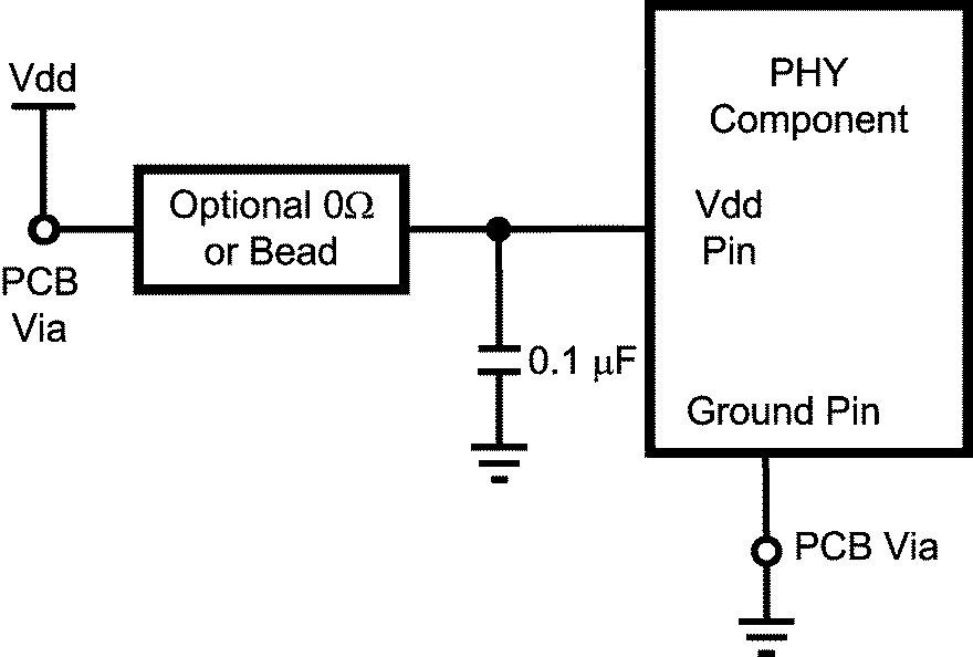
The device Vdd supply pins should be bypassed with low impedance 0.1-μF surface mount capacitors. To reduce EMI, the capacitors should be places as close as possible to the component Vdd supply pins, preferably between the supply pins and the vias connecting to the power plane. In some systems it may be desirable to add 0-Ω resistors in series with supply pins, as the resistor pads provide flexibility if adding EMI beads becomes necessary to meet system level certification testing requirements. (See Figure 7-1) It is recommended the PCB have at least one solid ground plane and one solid Vdd plane to provide a low impedance power source to the component. This also provides a low impedance return path for non-differential digital MII and clock signals. A 10-μF capacitor should also be placed near the PHY component for local bulk bypassing between the Vdd and ground planes.
 Figure 7-1 Vdd Bypass Layout