SNLS484H February 2015 – June 2024 DP83867CR , DP83867IR
PRODUCTION DATA
- 1
- 1 Features
- 2 Applications
- 3 Description
- 4 Device Comparison
- 5 Pin Configuration and Functions
-
6 Specifications
- 6.1 Absolute Maximum Ratings
- 6.2 ESD Ratings
- 6.3 Recommended Operating Conditions
- 6.4 Thermal Information
- 6.5 Electrical Characteristics
- 6.6 Power-Up Timing
- 6.7 Reset Timing
- 6.8 MII Serial Management Timing
- 6.9 RGMII Timing
- 6.10 GMII Transmit Timing
- 6.11 GMII Receive Timing
- 6.12 100Mbps MII Transmit Timing
- 6.13 100Mbps MII Receive Timing #GUID-033E0939-17C5-4DC1-9C2C-A3998C85D8B1/SNLS4845065
- 6.14 10Mbps MII Transmit Timing
- 6.15 10Mbps MII Receive Timing
- 6.16 DP83867IR/CR Start of Frame Detection Timing
- 6.17 Timing Diagrams
- 6.18 Typical Characteristics
-
7 Detailed Description
- 7.1 Overview
- 7.2 Functional Block Diagram
- 7.3 Feature Description
- 7.4
Device Functional Modes
- 7.4.1 MAC Interfaces
- 7.4.2
Serial Management Interface
- 7.4.2.1
Extended Address Space Access
- 7.4.2.1.1 Write Address Operation
- 7.4.2.1.2 Read Address Operation
- 7.4.2.1.3 Write (No Post Increment) Operation
- 7.4.2.1.4 Read (No Post Increment) Operation
- 7.4.2.1.5 Write (Post Increment) Operation
- 7.4.2.1.6 Read (Post Increment) Operation
- 7.4.2.1.7 Example of Read Operation Using Indirect Register Access
- 7.4.2.1.8 Example of Write Operation Using Indirect Register Access
- 7.4.2.1
Extended Address Space Access
- 7.4.3
Auto-Negotiation
- 7.4.3.1 Speed and Duplex Selection - Priority Resolution
- 7.4.3.2 Master and Slave Resolution
- 7.4.3.3 Pause and Asymmetrical Pause Resolution
- 7.4.3.4 Next Page Support
- 7.4.3.5 Parallel Detection
- 7.4.3.6 Restart Auto-Negotiation
- 7.4.3.7 Enabling Auto-Negotiation Through Software
- 7.4.3.8 Auto-Negotiation Complete Time
- 7.4.3.9 Auto-MDIX Resolution
- 7.4.4 Loopback Mode
- 7.4.5 BIST Configuration
- 7.4.6 Cable Diagnostics
- 7.5 Programming
- 7.6
Register Maps
- 7.6.1 Basic Mode Control Register (BMCR)
- 7.6.2 Basic Mode Status Register (BMSR)
- 7.6.3 PHY Identifier Register #1 (PHYIDR1)
- 7.6.4 PHY Identifier Register #2 (PHYIDR2)
- 7.6.5 Auto-Negotiation Advertisement Register (ANAR)
- 7.6.6 Auto-Negotiation Link Partner Ability Register (ANLPAR) (BASE Page)
- 7.6.7 Auto-Negotiate Expansion Register (ANER)
- 7.6.8 Auto-Negotiation Next Page Transmit Register (ANNPTR)
- 7.6.9 Auto-Negotiation Next Page Receive Register (ANNPRR)
- 7.6.10 1000BASE-T Configuration Register (CFG1)
- 7.6.11 Status Register 1 (STS1)
- 7.6.12 Extended Register Addressing
- 7.6.13 1000BASE-T Status Register (1KSCR)
- 7.6.14 PHY Control Register (PHYCR)
- 7.6.15 PHY Status Register (PHYSTS)
- 7.6.16 MII Interrupt Control Register (MICR)
- 7.6.17 Interrupt Status Register (ISR)
- 7.6.18 Configuration Register 2 (CFG2)
- 7.6.19 Receiver Error Counter Register (RECR)
- 7.6.20 BIST Control Register (BISCR)
- 7.6.21 Status Register 2 (STS2)
- 7.6.22 LED Configuration Register 1 (LEDCR1)
- 7.6.23 LED Configuration Register 2 (LEDCR2)
- 7.6.24 LED Configuration Register (LEDCR3)
- 7.6.25 Configuration Register 3 (CFG3)
- 7.6.26 Control Register (CTRL)
- 7.6.27 Testmode Channel Control (TMCH_CTRL)
- 7.6.28 Robust Auto MDIX Timer Configuration Register (AMDIX_TMR_CFG)
- 7.6.29 Fast Link Drop Configuration Register (FLD_CFG)
- 7.6.30 Fast Link Drop Threshold Configuration Register (FLD_THR_CFG)
- 7.6.31 Configuration Register 4 (CFG4)
- 7.6.32 RGMII Control Register (RGMIICTL)
- 7.6.33 RGMII Control Register 2 (RGMIICTL2)
- 7.6.34 100BASE-TX Configuration (100CR)
- 7.6.35 Viterbi Module Configuration (VTM_CFG)
- 7.6.36 Skew FIFO Status (SKEW_FIFO)
- 7.6.37 Strap Configuration Status Register 1 (STRAP_STS1)
- 7.6.38 Strap Configuration Status Register 2 (STRAP_STS2)
- 7.6.39 BIST Control and Status Register 1 (BICSR1)
- 7.6.40 BIST Control and Status Register 2 (BICSR2)
- 7.6.41 BIST Control and Status Register 3 (BICSR3)
- 7.6.42 BIST Control and Status Register 4 (BICSR4)
- 7.6.43 Configuration for Receiver's Equalizer (CRE)
- 7.6.44 RGMII Delay Control Register (RGMIIDCTL)
- 7.6.45 ANA_LD_TXG_FINE_GAINSEL_AB (ALTFGAB)
- 7.6.46 ANA_LD_TXG_FINE_GAINSEL_CD (ALTFGCD)
- 7.6.47 ANA_LD_FILTER_TUNE_AB (ALFTAB)
- 7.6.48 ANA_LD_FILTER_TUNE_CD (ALFTCD)
- 7.6.49 Configuration of Receiver's LPF (CRLPF)
- 7.6.50 Enable Control of Receiver's Equalizer (ECRE)
- 7.6.51 PLL Clock-out Control Register (PLLCTL)
- 7.6.52 Sync FIFO Control (SYNC_FIFO_CTRL)
- 7.6.53 Loopback Configuration Register (LOOPCR)
- 7.6.54 DSP Configuration (DSP_CONFIG)
- 7.6.55 DSP Feedforward Equalizer Configuration (DSP_FFE_CFG)
- 7.6.56 Receive Configuration Register (RXFCFG)
- 7.6.57 Receive Status Register (RXFSTS)
- 7.6.58 Pattern Match Data Register 1 (RXFPMD1)
- 7.6.59 Pattern Match Data Register 2 (RXFPMD2)
- 7.6.60 Pattern Match Data Register 3 (RXFPMD3)
- 7.6.61 SecureOn Pass Register 2 (RXFSOP1)
- 7.6.62 SecureOn Pass Register 2 (RXFSOP2)
- 7.6.63 SecureOn Pass Register 3 (RXFSOP3)
- 7.6.64 Receive Pattern Register 1 (RXFPAT1)
- 7.6.65 Receive Pattern Register 2 (RXFPAT2)
- 7.6.66 Receive Pattern Register 3 (RXFPAT3)
- 7.6.67 Receive Pattern Register 4 (RXFPAT4)
- 7.6.68 Receive Pattern Register 5 (RXFPAT5)
- 7.6.69 Receive Pattern Register 6 (RXFPAT6)
- 7.6.70 Receive Pattern Register 7 (RXFPAT7)
- 7.6.71 Receive Pattern Register 8 (RXFPAT8)
- 7.6.72 Receive Pattern Register 9 (RXFPAT9)
- 7.6.73 Receive Pattern Register 10 (RXFPAT10)
- 7.6.74 Receive Pattern Register 11 (RXFPAT11)
- 7.6.75 Receive Pattern Register 12 (RXFPAT12)
- 7.6.76 Receive Pattern Register 13 (RXFPAT13)
- 7.6.77 Receive Pattern Register 14 (RXFPAT14)
- 7.6.78 Receive Pattern Register 15 (RXFPAT15)
- 7.6.79 Receive Pattern Register 16 (RXFPAT16)
- 7.6.80 Receive Pattern Register 17 (RXFPAT17)
- 7.6.81 Receive Pattern Register 18 (RXFPAT18)
- 7.6.82 Receive Pattern Register 19 (RXFPAT19)
- 7.6.83 Receive Pattern Register 20 (RXFPAT20)
- 7.6.84 Receive Pattern Register 21 (RXFPAT21)
- 7.6.85 Receive Pattern Register 22 (RXFPAT22)
- 7.6.86 Receive Pattern Register 23 (RXFPAT23)
- 7.6.87 Receive Pattern Register 24 (RXFPAT24)
- 7.6.88 Receive Pattern Register 25 (RXFPAT25)
- 7.6.89 Receive Pattern Register 26 (RXFPAT26)
- 7.6.90 Receive Pattern Register 27 (RXFPAT27)
- 7.6.91 Receive Pattern Register 28 (RXFPAT28)
- 7.6.92 Receive Pattern Register 29 (RXFPAT29)
- 7.6.93 Receive Pattern Register 30 (RXFPAT30)
- 7.6.94 Receive Pattern Register 31 (RXFPAT31)
- 7.6.95 Receive Pattern Register 32 (RXFPAT32)
- 7.6.96 Receive Pattern Byte Mask Register 1 (RXFPBM1)
- 7.6.97 Receive Pattern Byte Mask Register 2 (RXFPBM2)
- 7.6.98 Receive Pattern Byte Mask Register 3 (RXFPBM3)
- 7.6.99 Receive Pattern Byte Mask Register 4 (RXFPBM4)
- 7.6.100 Receive Pattern Control (RXFPATC)
- 7.6.101 I/O Configuration (IO_MUX_CFG)
- 7.6.102 GPIO Mux Control Register 1 (GPIO_MUX_CTRL1)
- 7.6.103 GPIO Mux Control Register 2 (GPIO_MUX_CTRL2)
- 7.6.104 GPIO Mux Control Register (GPIO_MUX_CTRL)
- 7.6.105 TDR General Configuration Register 1 (TDR_GEN_CFG1)
- 7.6.106 TDR Peak Locations Register 1 (TDR_PEAKS_LOC_1)
- 7.6.107 TDR Peak Locations Register 2 (TDR_PEAKS_LOC_2)
- 7.6.108 TDR Peak Locations Register 3 (TDR_PEAKS_LOC_3)
- 7.6.109 TDR Peak Locations Register 4 (TDR_PEAKS_LOC_4)
- 7.6.110 TDR Peak Locations Register 5 (TDR_PEAKS_LOC_5)
- 7.6.111 TDR Peak Locations Register 6 (TDR_PEAKS_LOC_6)
- 7.6.112 TDR Peak Locations Register 7 (TDR_PEAKS_LOC_7)
- 7.6.113 TDR Peak Locations Register 8 (TDR_PEAKS_LOC_8)
- 7.6.114 TDR Peak Locations Register 9 (TDR_PEAKS_LOC_9)
- 7.6.115 TDR Peak Locations Register 10 (TDR_PEAKS_LOC_10)
- 7.6.116 TDR Peak Amplitudes Register 1 (TDR_PEAKS_AMP_1)
- 7.6.117 TDR Peak Amplitudes Register 2 (TDR_PEAKS_AMP_2)
- 7.6.118 TDR Peak Amplitudes Register 3 (TDR_PEAKS_AMP_3)
- 7.6.119 TDR Peak Amplitudes Register 4 (TDR_PEAKS_AMP_4)
- 7.6.120 TDR Peak Amplitudes Register 5 (TDR_PEAKS_AMP_5)
- 7.6.121 TDR Peak Amplitudes Register 6 (TDR_PEAKS_AMP_6)
- 7.6.122 TDR Peak Amplitudes Register 7 (TDR_PEAKS_AMP_7)
- 7.6.123 TDR Peak Amplitudes Register 8 (TDR_PEAKS_AMP_8)
- 7.6.124 TDR Peak Amplitudes Register 9 (TDR_PEAKS_AMP_9)
- 7.6.125 TDR Peak Amplitudes Register 10 (TDR_PEAKS_AMP_10)
- 7.6.126 TDR General Status (TDR_GEN_STATUS)
- 7.6.127 TDR Peak Sign AB (TDR_PEAK_SIGN_A_B)
- 7.6.128 TDR Peak Sign CD (TDR_PEAK_SIGN_C_D)
- 8 Application and Implementation
- 9 Device and Documentation Support
- 10Revision History
- 11Mechanical, Packaging, and Orderable Information
Package Options
Refer to the PDF data sheet for device specific package drawings
Mechanical Data (Package|Pins)
- RGZ|48
Thermal pad, mechanical data (Package|Pins)
- RGZ|48
Orderable Information
8.4.1.5 PCB Layer Stacking
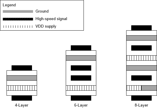
To meet signal integrity and performance requirements, at minimum a 4-layer PCB should be used. However a 6-layer board is recommended. See Figure 8-12 for the recommended layer stack ups for 4, 6 and 8-layer boards. These are recommendations not requirements, other configurations can be used as per system requirements.
 Figure 8-12 Recommended Layer Stack Up
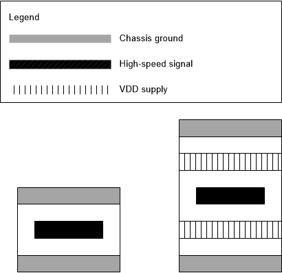
Within a PCB, it may be desirable to run traces using different methods, microstrip vs. stripline, depending on the location of the signal on the PCB. For example, it may be desirable to change layer stacking where an isolated chassis ground plane is used. Figure 8-13 illustrates alternative PCB stacking options.
 Figure 8-13 Alternative Layer Stack Up