SNLS504E October 2015 – May 2024 DP83867CS , DP83867E , DP83867IS
PRODUCTION DATA
- 1
- 1 Features
- 2 Applications
- 3 Description
- 4 Device Comparison
- 5 Pin Configuration and Functions
-
6 Specifications
- 6.1 Absolute Maximum Ratings
- 6.2 ESD Ratings
- 6.3 Recommended Operating Conditions
- 6.4 Thermal Information
- 6.5 Electrical Characteristics
- 6.6 Power-Up Timing
- 6.7 Reset Timing
- 6.8 MII Serial Management Timing
- 6.9 SGMII Timing
- 6.10 RGMII Timing
- 6.11 DP83867E Start of Frame Detection Timing
- 6.12 DP83867IS/CS Start of Frame Detection Timing
- 6.13 Timing Diagrams
- 6.14 Typical Characteristics
-
7 Detailed Description
- 7.1 Overview
- 7.2 Functional Block Diagram
- 7.3 Feature Description
- 7.4
Device Functional Modes
- 7.4.1 MAC Interfaces
- 7.4.2
Serial Management Interface
- 7.4.2.1
Extended Address Space Access
- 7.4.2.1.1 Write Address Operation
- 7.4.2.1.2 Read Address Operation
- 7.4.2.1.3 Write (No Post Increment) Operation
- 7.4.2.1.4 Read (No Post Increment) Operation
- 7.4.2.1.5 Write (Post Increment) Operation
- 7.4.2.1.6 Read (Post Increment) Operation
- 7.4.2.1.7 Example of Read Operation Using Indirect Register Access
- 7.4.2.1.8 Example of Write Operation Using Indirect Register Access
- 7.4.2.1
Extended Address Space Access
- 7.4.3
Auto-Negotiation
- 7.4.3.1 Speed and Duplex Selection - Priority Resolution
- 7.4.3.2 Master and Slave Resolution
- 7.4.3.3 Pause and Asymmetrical Pause Resolution
- 7.4.3.4 Next Page Support
- 7.4.3.5 Parallel Detection
- 7.4.3.6 Restart Auto-Negotiation
- 7.4.3.7 Enabling Auto-Negotiation Through Software
- 7.4.3.8 Auto-Negotiation Complete Time
- 7.4.3.9 Auto-MDIX Resolution
- 7.4.4 Loopback Mode
- 7.4.5 BIST Configuration
- 7.4.6 Cable Diagnostics
- 7.5 Programming
- 7.6
Register Maps
- 7.6.1 Basic Mode Control Register (BMCR)
- 7.6.2 Basic Mode Status Register (BMSR)
- 7.6.3 PHY Identifier Register #1 (PHYIDR1)
- 7.6.4 PHY Identifier Register #2 (PHYIDR2)
- 7.6.5 Auto-Negotiation Advertisement Register (ANAR)
- 7.6.6 Auto-Negotiation Link Partner Ability Register (ANLPAR) (BASE Page)
- 7.6.7 Auto-Negotiate Expansion Register (ANER)
- 7.6.8 Auto-Negotiation Next Page Transmit Register (ANNPTR)
- 7.6.9 Auto-Negotiation Next Page Receive Register (ANNPRR)
- 7.6.10 1000BASE-T Configuration Register (CFG1)
- 7.6.11 Status Register 1 (STS1)
- 7.6.12 Extended Register Addressing
- 7.6.13 1000BASE-T Status Register (1KSCR)
- 7.6.14 PHY Control Register (PHYCR)
- 7.6.15 PHY Status Register (PHYSTS)
- 7.6.16 MII Interrupt Control Register (MICR)
- 7.6.17 Interrupt Status Register (ISR)
- 7.6.18 Configuration Register 2 (CFG2)
- 7.6.19 Receiver Error Counter Register (RECR)
- 7.6.20 BIST Control Register (BISCR)
- 7.6.21 Status Register 2 (STS2)
- 7.6.22 LED Configuration Register 1 (LEDCR1)
- 7.6.23 LED Configuration Register 2 (LEDCR2)
- 7.6.24 LED Configuration Register (LEDCR3)
- 7.6.25 Configuration Register 3 (CFG3)
- 7.6.26 Control Register (CTRL)
- 7.6.27 Testmode Channel Control (TMCH_CTRL)
- 7.6.28 Robust Auto MDIX Timer Configuration Register (AMDIX_TMR_CFG)
- 7.6.29 Fast Link Drop Configuration Register (FLD_CFG)
- 7.6.30 Fast Link Drop Threshold Configuration Register (FLD_THR_CFG)
- 7.6.31 Configuration Register 4 (CFG4)
- 7.6.32 RGMII Control Register (RGMIICTL)
- 7.6.33 RGMII Control Register 2 (RGMIICTL2)
- 7.6.34 SGMII Auto-Negotiation Status (SGMII_ANEG_STS)
- 7.6.35 100BASE-TX Configuration (100CR)
- 7.6.36 Viterbi Module Configuration (VTM_CFG)
- 7.6.37 Skew FIFO Status (SKEW_FIFO)
- 7.6.38 Strap Configuration Status Register 1 (STRAP_STS1)
- 7.6.39 Strap Configuration Status Register 2 (STRAP_STS2)
- 7.6.40 BIST Control and Status Register 1 (BICSR1)
- 7.6.41 BIST Control and Status Register 2 (BICSR2)
- 7.6.42 BIST Control and Status Register 3 (BICSR3)
- 7.6.43 BIST Control and Status Register 4 (BICSR4)
- 7.6.44 Configuration for Receiver's Equalizer (CRE)
- 7.6.45 RGMII Delay Control Register (RGMIIDCTL)
- 7.6.46 ANA_LD_TXG_FINE_GAINSEL_AB (ALTFGAB)
- 7.6.47 ANA_LD_TXG_FINE_GAINSEL_CD (ALTFGCD)
- 7.6.48 ANA_LD_FILTER_TUNE_AB (ALFTAB)
- 7.6.49 ANA_LD_FILTER_TUNE_CD (ALFTCD)
- 7.6.50 Configuration of Receiver's LPF (CRLPF)
- 7.6.51 Enable Control of Receiver's Equalizer (ECRE)
- 7.6.52 PLL Clock-out Control Register (PLLCTL)
- 7.6.53 SGMII Control Register 1 (SGMIICTL1)
- 7.6.54 Sync FIFO Control (SYNC_FIFO_CTRL)
- 7.6.55 Loopback Configuration Register (LOOPCR)
- 7.6.56 DSP Configuration (DSP_CONFIG)
- 7.6.57 DSP Feedforward Equalizer Configuration (DSP_FFE_CFG)
- 7.6.58 Receive Configuration Register (RXFCFG)
- 7.6.59 Receive Status Register (RXFSTS)
- 7.6.60 Pattern Match Data Register 1 (RXFPMD1)
- 7.6.61 Pattern Match Data Register 2 (RXFPMD2)
- 7.6.62 Pattern Match Data Register 3 (RXFPMD3)
- 7.6.63 SecureOn Pass Register 2 (RXFSOP1)
- 7.6.64 SecureOn Pass Register 2 (RXFSOP2)
- 7.6.65 SecureOn Pass Register 3 (RXFSOP3)
- 7.6.66 Receive Pattern Register 1 (RXFPAT1)
- 7.6.67 Receive Pattern Register 2 (RXFPAT2)
- 7.6.68 Receive Pattern Register 3 (RXFPAT3)
- 7.6.69 Receive Pattern Register 4 (RXFPAT4)
- 7.6.70 Receive Pattern Register 5 (RXFPAT5)
- 7.6.71 Receive Pattern Register 6 (RXFPAT6)
- 7.6.72 Receive Pattern Register 7 (RXFPAT7)
- 7.6.73 Receive Pattern Register 8 (RXFPAT8)
- 7.6.74 Receive Pattern Register 9 (RXFPAT9)
- 7.6.75 Receive Pattern Register 10 (RXFPAT10)
- 7.6.76 Receive Pattern Register 11 (RXFPAT11)
- 7.6.77 Receive Pattern Register 12 (RXFPAT12)
- 7.6.78 Receive Pattern Register 13 (RXFPAT13)
- 7.6.79 Receive Pattern Register 14 (RXFPAT14)
- 7.6.80 Receive Pattern Register 15 (RXFPAT15)
- 7.6.81 Receive Pattern Register 16 (RXFPAT16)
- 7.6.82 Receive Pattern Register 17 (RXFPAT17)
- 7.6.83 Receive Pattern Register 18 (RXFPAT18)
- 7.6.84 Receive Pattern Register 19 (RXFPAT19)
- 7.6.85 Receive Pattern Register 20 (RXFPAT20)
- 7.6.86 Receive Pattern Register 21 (RXFPAT21)
- 7.6.87 Receive Pattern Register 22 (RXFPAT22)
- 7.6.88 Receive Pattern Register 23 (RXFPAT23)
- 7.6.89 Receive Pattern Register 24 (RXFPAT24)
- 7.6.90 Receive Pattern Register 25 (RXFPAT25)
- 7.6.91 Receive Pattern Register 26 (RXFPAT26)
- 7.6.92 Receive Pattern Register 27 (RXFPAT27)
- 7.6.93 Receive Pattern Register 28 (RXFPAT28)
- 7.6.94 Receive Pattern Register 29 (RXFPAT29)
- 7.6.95 Receive Pattern Register 30 (RXFPAT30)
- 7.6.96 Receive Pattern Register 31 (RXFPAT31)
- 7.6.97 Receive Pattern Register 32 (RXFPAT32)
- 7.6.98 Receive Pattern Byte Mask Register 1 (RXFPBM1)
- 7.6.99 Receive Pattern Byte Mask Register 2 (RXFPBM2)
- 7.6.100 Receive Pattern Byte Mask Register 3 (RXFPBM3)
- 7.6.101 Receive Pattern Byte Mask Register 4 (RXFPBM4)
- 7.6.102 Receive Pattern Control (RXFPATC)
- 7.6.103 10M SGMII Configuration (10M_SGMII_CFG)
- 7.6.104 I/O Configuration (IO_MUX_CFG)
- 7.6.105 GPIO Mux Control Register (GPIO_MUX_CTRL)
- 7.6.106 TDR General Configuration Register 1 (TDR_GEN_CFG1)
- 7.6.107 TDR Peak Locations Register 1 (TDR_PEAKS_LOC_1)
- 7.6.108 TDR Peak Locations Register 2 (TDR_PEAKS_LOC_2)
- 7.6.109 TDR Peak Locations Register 3 (TDR_PEAKS_LOC_3)
- 7.6.110 TDR Peak Locations Register 4 (TDR_PEAKS_LOC_4)
- 7.6.111 TDR Peak Locations Register 5 (TDR_PEAKS_LOC_5)
- 7.6.112 TDR Peak Locations Register 6 (TDR_PEAKS_LOC_6)
- 7.6.113 TDR Peak Locations Register 7 (TDR_PEAKS_LOC_7)
- 7.6.114 TDR Peak Locations Register 8 (TDR_PEAKS_LOC_8)
- 7.6.115 TDR Peak Locations Register 9 (TDR_PEAKS_LOC_9)
- 7.6.116 TDR Peak Locations Register 10 (TDR_PEAKS_LOC_10)
- 7.6.117 TDR Peak Amplitudes Register 1 (TDR_PEAKS_AMP_1)
- 7.6.118 TDR Peak Amplitudes Register 2 (TDR_PEAKS_AMP_2)
- 7.6.119 TDR Peak Amplitudes Register 3 (TDR_PEAKS_AMP_3)
- 7.6.120 TDR Peak Amplitudes Register 4 (TDR_PEAKS_AMP_4)
- 7.6.121 TDR Peak Amplitudes Register 5 (TDR_PEAKS_AMP_5)
- 7.6.122 TDR Peak Amplitudes Register 6 (TDR_PEAKS_AMP_6)
- 7.6.123 TDR Peak Amplitudes Register 7 (TDR_PEAKS_AMP_7)
- 7.6.124 TDR Peak Amplitudes Register 8 (TDR_PEAKS_AMP_8)
- 7.6.125 TDR Peak Amplitudes Register 9 (TDR_PEAKS_AMP_9)
- 7.6.126 TDR Peak Amplitudes Register 10 (TDR_PEAKS_AMP_10)
- 7.6.127 TDR General Status (TDR_GEN_STATUS)
- 7.6.128 TDR Peak Sign AB (TDR_PEAK_SIGN_A_B)
- 7.6.129 TDR Peak Sign CD (TDR_PEAK_SIGN_C_D)
- 7.6.130 Programmable Gain Register (PROG_GAIN)
- 7.6.131 MMD3 PCS Control Register (MMD3_PCS_CTRL)
- 8 Application and Implementation
- 9 Device and Documentation Support
- 10Revision History
- 11Mechanical, Packaging, and Orderable Information
Package Options
Refer to the PDF data sheet for device specific package drawings
Mechanical Data (Package|Pins)
- RGZ|48
Thermal pad, mechanical data (Package|Pins)
- RGZ|48
Orderable Information
7.5.4 PHY Address Configuration
The DP83867 can be set to respond to any of 16 possible PHY addresses through strap pins. The information is latched into the device at a device power up or hardware reset. Each DP83867 or port sharing an MDIO bus in a system must have a unique physical address. The DP83867 supports PHY address strapping values 0 (<0000>) through 15 (<1111>).
For further detail relating to the latch-in timing requirements of the PHY Address pins, as well as the other hardware configuration pins, refer to Section 7.5.5.
Based on the default strap configuration of PHY_ADD[3:0], the DP83867 PHY address initializes to 0x00 without any external strap configuration.
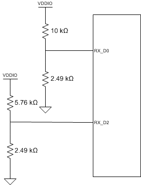
Refer to Figure 7-13 for an example of a PHY address connection to external components. In this example, the pins are configured as follows: RX_D2 = Strap Mode 3 and RX_D0 = Strap Mode 2. Therefore, the PHY address strapping results in address 1001 (09h).
 Figure 7-13 PHY Address Strapping Example
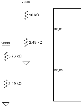
When operating in SGMII mode, dummy straps must be added to provide a balanced load for the SGMII differential pairs. Therefore, for SGMII applications with the straps shown in Figure 7-13, the corresponding connections for RX_D1 and RX_D3 are shown in Figure 7-14.
 Figure 7-14 PHY Address Strapping Example for SGMII