SNLS614C September   2018  – April 2024 DP83869HM

PRODUCTION DATA  

  1.   1
  2. Features
  3. Applications
  4. Description
  5. Device Comparison
  6. Pin Configuration and Functions
  7. Specifications
    1. 6.1 Absolute Maximum Ratings
    2. 6.2 ESD Ratings
    3. 6.3 Recommended Operating Conditions
    4. 6.4 Thermal Information
    5. 6.5 Electrical Characteristics
    6. 6.6 Timing Requirements
    7. 6.7 Timing Diagrams
    8. 6.8 Typical Characteristics
  8. Detailed Description
    1. 7.1 Overview
    2. 7.2 Functional Block Diagram
    3. 7.3 Feature Description
      1. 7.3.1  WoL (Wake-on-LAN) Packet Detection
        1. 7.3.1.1 Magic Packet Structure
        2. 7.3.1.2 Wake-on-LAN Configuration and Status
      2. 7.3.2  Start of Frame Detect for IEEE 1588 Time Stamp
        1. 7.3.2.1 SFD Latency Variation and Determinism
          1. 7.3.2.1.1 1000Mb SFD Variation in Master Mode
          2. 7.3.2.1.2 1000Mb SFD Variation in Slave Mode
          3. 7.3.2.1.3 100-Mb SFD Variation
      3. 7.3.3  Clock Output
      4. 7.3.4  Loopback Mode
        1. 7.3.4.1 Near-End Loopback
          1. 7.3.4.1.1 MII Loopback
          2. 7.3.4.1.2 PCS Loopback
          3. 7.3.4.1.3 Digital Loopback
          4. 7.3.4.1.4 Analog Loopback
          5. 7.3.4.1.5 External Loopback
          6. 7.3.4.1.6 Far-End (Reverse) Loopback
        2.       37
      5. 7.3.5  BIST Configuration
      6. 7.3.6  Interrupt
      7. 7.3.7  Power-Saving Modes
        1. 7.3.7.1 IEEE Power Down
        2. 7.3.7.2 Active Sleep
        3. 7.3.7.3 Passive Sleep
      8. 7.3.8  Mirror Mode
      9. 7.3.9  Speed Optimization
      10. 7.3.10 Cable Diagnostics
        1. 7.3.10.1 TDR
      11. 7.3.11 Fast Link Drop
      12. 7.3.12 Jumbo Frames
    4. 7.4 Device Functional Modes
      1. 7.4.1  Copper Ethernet
        1. 7.4.1.1 1000BASE-T
        2. 7.4.1.2 100BASE-TX
        3. 7.4.1.3 10BASE-Te
      2. 7.4.2  Fiber Ethernet
        1. 7.4.2.1 1000BASE-X
        2. 7.4.2.2 100BASE-FX
      3. 7.4.3  Serial GMII (SGMII)
      4. 7.4.4  Reduced GMII (RGMII)
        1. 7.4.4.1 1000Mbps Mode Operation
        2. 7.4.4.2 1000Mbps Mode Timing
        3. 7.4.4.3 10 and 100Mbps Mode
      5. 7.4.5  Media Independent Interface (MII)
      6. 7.4.6  Bridge Modes
        1. 7.4.6.1 RGMII-to-SGMII Mode
        2. 7.4.6.2 SGMII-to-RGMII Mode
        3.       67
      7. 7.4.7  Media Convertor Mode
      8. 7.4.8  Register Configuration for Operational Modes
        1. 7.4.8.1 RGMII-to-Copper Ethernet Mode
        2. 7.4.8.2 RGMII-to-1000Base-X Mode
        3. 7.4.8.3 RGMII-to-100Base-FX Mode
        4. 7.4.8.4 RGMII-to-SGMII Bridge Mode
        5. 7.4.8.5 1000M Media Convertor Mode
        6. 7.4.8.6 100M Media Convertor Mode
        7. 7.4.8.7 SGMII-to-Copper Ethernet Mode
      9. 7.4.9  Serial Management Interface
        1. 7.4.9.1 Extended Register Space Access
          1. 7.4.9.1.1 Read (No Post Increment) Operation
          2. 7.4.9.1.2 Write (No Post Increment) Operation
      10. 7.4.10 Auto-Negotiation
        1. 7.4.10.1 Speed and Duplex Selection - Priority Resolution
        2. 7.4.10.2 Master and Slave Resolution
        3. 7.4.10.3 Pause and Asymmetrical Pause Resolution
        4. 7.4.10.4 Next Page Support
        5. 7.4.10.5 Parallel Detection
        6. 7.4.10.6 Restart Auto-Negotiation
        7. 7.4.10.7 Enabling Auto-Negotiation Through Software
        8. 7.4.10.8 Auto-Negotiation Complete Time
        9. 7.4.10.9 Auto-MDIX Resolution
    5. 7.5 Programming
      1. 7.5.1 Strap Configuration
        1. 7.5.1.1 Straps for PHY Address
        2. 7.5.1.2 Strap for DP83869HM Functional Mode Selection
        3. 7.5.1.3 LED Default Configuration Based on Device Mode
        4. 7.5.1.4 Straps for RGMII/SGMII to Copper
        5. 7.5.1.5 Straps for RGMII to 1000Base-X
        6. 7.5.1.6 Straps for RGMII to 100Base-FX
        7. 7.5.1.7 Straps for Bridge Mode (SGMII-RGMII)
        8. 7.5.1.8 Straps for 100M Media Convertor
        9. 7.5.1.9 Straps for 1000M Media Convertor
      2. 7.5.2 LED Configuration
      3. 7.5.3 Reset Operation
        1. 7.5.3.1 Hardware Reset
        2. 7.5.3.2 IEEE Software Reset
        3. 7.5.3.3 Global Software Reset
        4. 7.5.3.4 Global Software Restart
    6. 7.6 Register Maps
      1. 7.6.1 DP83869 Registers
  9. Application and Implementation
    1. 8.1 Application Information
    2. 8.2 Typical Applications
      1. 8.2.1 Copper Ethernet Typical Application
        1. 8.2.1.1 Design Requirements
        2. 8.2.1.2 Detailed Design Procedure
          1. 8.2.1.2.1 Clock Input
            1. 8.2.1.2.1.1 Crystal Recommendations
            2. 8.2.1.2.1.2 External Clock Source Recommendation
          2. 8.2.1.2.2 Magnetics Requirements
            1. 8.2.1.2.2.1 Magnetics Connection
        3. 8.2.1.3 Application Curves
      2. 8.2.2 Fiber Ethernet Typical Ethernet
        1. 8.2.2.1 Design Requirements
        2. 8.2.2.2 Detailed Design Procedure
          1. 8.2.2.2.1 Transceiver Connections
        3. 8.2.2.3 Application Curves
    3. 8.3 Power Supply Recommendations
      1. 8.3.1 Two-Supply Configuration
      2. 8.3.2 Three-Supply Configuration
    4. 8.4 Layout
      1. 8.4.1 Layout Guidelines
        1. 8.4.1.1 Signal Traces
          1. 8.4.1.1.1 MAC Interface Layout Guidelines
            1. 8.4.1.1.1.1 SGMII Layout Guidelines
            2. 8.4.1.1.1.2 RGMII Layout Guidelines
          2. 8.4.1.1.2 MDI Layout Guidelines
        2. 8.4.1.2 Return Path
        3. 8.4.1.3 Transformer Layout
        4. 8.4.1.4 Metal Pour
        5. 8.4.1.5 PCB Layer Stacking
      2. 8.4.2 Layout Example
  10. Device and Documentation Support
    1. 9.1 Documentation Support
      1. 9.1.1 Related Documentation
    2. 9.2 Receiving Notification of Documentation Updates
    3. 9.3 Support Resources
    4. 9.4 Trademarks
    5. 9.5 Electrostatic Discharge Caution
    6. 9.6 Glossary
  11. 10Revision History
  12. 11Mechanical, Packaging, and Orderable Information

Package Options

Mechanical Data (Package|Pins)
Thermal pad, mechanical data (Package|Pins)
Orderable Information

Description

The DP83869HM device is a robust, fully-featured gigabit physical layer (PHY) transceiver with integrated PMD sublayers that supports 10BASE-Te, 100BASE-TX and 1000BASE-T Ethernet protocols. The DP83869 also supports 1000BASE-X and 100BASE-FX fiber protocols. Optimized for ESD protection, the DP83869HM exceeds 8kV IEC 61000-4-2 (direct contact).This device interfaces to the MAC layer through reduced GMII (RGMII) and SGMII. In 100M mode, the device lets the designer use MII for lower latency. Programmable integrated termination impedance on RGMII/MII helps reduce system BOM.

The DP83869HM supports media conversion in unmanaged mode. In this mode, the DP83869HM can run 1000BASE-X-to-1000BASE-T and 100BASE-FX-to-100BASE-TX conversions.

The DP83869HM can also support bridge conversion from RGMII to SGMII and SGMII to RGMII. The DP83869HM is compliant to TSN standards and offers low latency.

The DP83869HM can also generate IEEE 1588 Sync Frame Detect indications to MAC. This can reduce the jitter in Time Synchronization and help the System account for asymmetric delays in Transmission and Reception of packets.

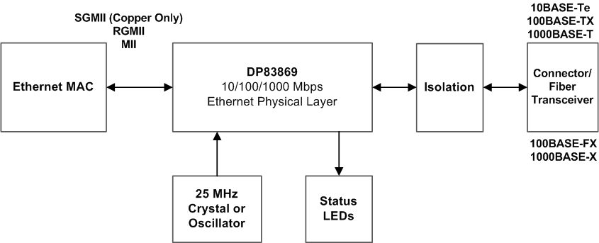
The standard Ethernet system block diagram is shown on the first page. Designers can also use the DP83869 in Media Convertor mode, in RGMII-to-SGMII Bridge applications, and in SGMII-RGMII Bridge applications.

Package Information
PART NUMBER PACKAGE (1) PACKAGE SIZE(2)
DP83869HM RGZ (VQFN, 48) 7mm × 7mm
DP83867E/IS/CS RGZ (VQFN, 48) 7mm × 7mm
DP83867IR/CR RGZ (VQFN, 48) 7mm × 7mm
For all available packages, see Section 11.
The package size (length × width) is a nominal value and includes pins, where applicable.
DP83869HM Standard Ethernet System Block Diagram Standard Ethernet System Block Diagram
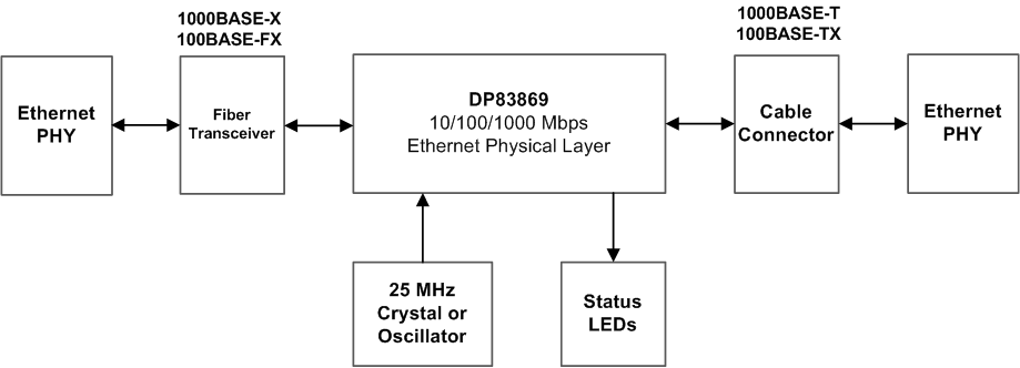
DP83869HM Media Convertor System Block
            Diagram Figure 3-1 Media Convertor System Block Diagram
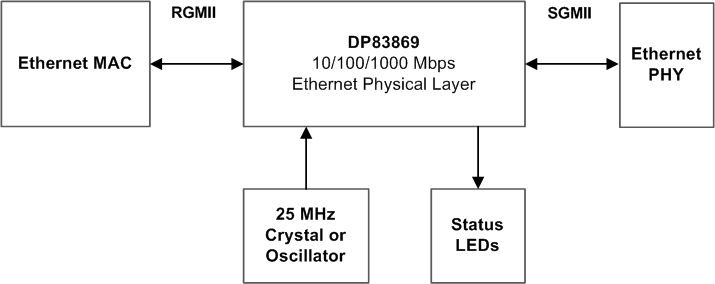
DP83869HM RGMII-SGMII Bridge System Block
            Diagram Figure 3-2 RGMII-SGMII Bridge System Block Diagram
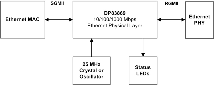
DP83869HM SGMII-RGMII Bridge System Block
            Diagram Figure 3-3 SGMII-RGMII Bridge System Block Diagram