SNLS614C September   2018  – April 2024 DP83869HM

PRODUCTION DATA  

  1.   1
  2. Features
  3. Applications
  4. Description
  5. Device Comparison
  6. Pin Configuration and Functions
  7. Specifications
    1. 6.1 Absolute Maximum Ratings
    2. 6.2 ESD Ratings
    3. 6.3 Recommended Operating Conditions
    4. 6.4 Thermal Information
    5. 6.5 Electrical Characteristics
    6. 6.6 Timing Requirements
    7. 6.7 Timing Diagrams
    8. 6.8 Typical Characteristics
  8. Detailed Description
    1. 7.1 Overview
    2. 7.2 Functional Block Diagram
    3. 7.3 Feature Description
      1. 7.3.1  WoL (Wake-on-LAN) Packet Detection
        1. 7.3.1.1 Magic Packet Structure
        2. 7.3.1.2 Wake-on-LAN Configuration and Status
      2. 7.3.2  Start of Frame Detect for IEEE 1588 Time Stamp
        1. 7.3.2.1 SFD Latency Variation and Determinism
          1. 7.3.2.1.1 1000Mb SFD Variation in Master Mode
          2. 7.3.2.1.2 1000Mb SFD Variation in Slave Mode
          3. 7.3.2.1.3 100-Mb SFD Variation
      3. 7.3.3  Clock Output
      4. 7.3.4  Loopback Mode
        1. 7.3.4.1 Near-End Loopback
          1. 7.3.4.1.1 MII Loopback
          2. 7.3.4.1.2 PCS Loopback
          3. 7.3.4.1.3 Digital Loopback
          4. 7.3.4.1.4 Analog Loopback
          5. 7.3.4.1.5 External Loopback
          6. 7.3.4.1.6 Far-End (Reverse) Loopback
        2.       37
      5. 7.3.5  BIST Configuration
      6. 7.3.6  Interrupt
      7. 7.3.7  Power-Saving Modes
        1. 7.3.7.1 IEEE Power Down
        2. 7.3.7.2 Active Sleep
        3. 7.3.7.3 Passive Sleep
      8. 7.3.8  Mirror Mode
      9. 7.3.9  Speed Optimization
      10. 7.3.10 Cable Diagnostics
        1. 7.3.10.1 TDR
      11. 7.3.11 Fast Link Drop
      12. 7.3.12 Jumbo Frames
    4. 7.4 Device Functional Modes
      1. 7.4.1  Copper Ethernet
        1. 7.4.1.1 1000BASE-T
        2. 7.4.1.2 100BASE-TX
        3. 7.4.1.3 10BASE-Te
      2. 7.4.2  Fiber Ethernet
        1. 7.4.2.1 1000BASE-X
        2. 7.4.2.2 100BASE-FX
      3. 7.4.3  Serial GMII (SGMII)
      4. 7.4.4  Reduced GMII (RGMII)
        1. 7.4.4.1 1000Mbps Mode Operation
        2. 7.4.4.2 1000Mbps Mode Timing
        3. 7.4.4.3 10 and 100Mbps Mode
      5. 7.4.5  Media Independent Interface (MII)
      6. 7.4.6  Bridge Modes
        1. 7.4.6.1 RGMII-to-SGMII Mode
        2. 7.4.6.2 SGMII-to-RGMII Mode
        3.       67
      7. 7.4.7  Media Convertor Mode
      8. 7.4.8  Register Configuration for Operational Modes
        1. 7.4.8.1 RGMII-to-Copper Ethernet Mode
        2. 7.4.8.2 RGMII-to-1000Base-X Mode
        3. 7.4.8.3 RGMII-to-100Base-FX Mode
        4. 7.4.8.4 RGMII-to-SGMII Bridge Mode
        5. 7.4.8.5 1000M Media Convertor Mode
        6. 7.4.8.6 100M Media Convertor Mode
        7. 7.4.8.7 SGMII-to-Copper Ethernet Mode
      9. 7.4.9  Serial Management Interface
        1. 7.4.9.1 Extended Register Space Access
          1. 7.4.9.1.1 Read (No Post Increment) Operation
          2. 7.4.9.1.2 Write (No Post Increment) Operation
      10. 7.4.10 Auto-Negotiation
        1. 7.4.10.1 Speed and Duplex Selection - Priority Resolution
        2. 7.4.10.2 Master and Slave Resolution
        3. 7.4.10.3 Pause and Asymmetrical Pause Resolution
        4. 7.4.10.4 Next Page Support
        5. 7.4.10.5 Parallel Detection
        6. 7.4.10.6 Restart Auto-Negotiation
        7. 7.4.10.7 Enabling Auto-Negotiation Through Software
        8. 7.4.10.8 Auto-Negotiation Complete Time
        9. 7.4.10.9 Auto-MDIX Resolution
    5. 7.5 Programming
      1. 7.5.1 Strap Configuration
        1. 7.5.1.1 Straps for PHY Address
        2. 7.5.1.2 Strap for DP83869HM Functional Mode Selection
        3. 7.5.1.3 LED Default Configuration Based on Device Mode
        4. 7.5.1.4 Straps for RGMII/SGMII to Copper
        5. 7.5.1.5 Straps for RGMII to 1000Base-X
        6. 7.5.1.6 Straps for RGMII to 100Base-FX
        7. 7.5.1.7 Straps for Bridge Mode (SGMII-RGMII)
        8. 7.5.1.8 Straps for 100M Media Convertor
        9. 7.5.1.9 Straps for 1000M Media Convertor
      2. 7.5.2 LED Configuration
      3. 7.5.3 Reset Operation
        1. 7.5.3.1 Hardware Reset
        2. 7.5.3.2 IEEE Software Reset
        3. 7.5.3.3 Global Software Reset
        4. 7.5.3.4 Global Software Restart
    6. 7.6 Register Maps
      1. 7.6.1 DP83869 Registers
  9. Application and Implementation
    1. 8.1 Application Information
    2. 8.2 Typical Applications
      1. 8.2.1 Copper Ethernet Typical Application
        1. 8.2.1.1 Design Requirements
        2. 8.2.1.2 Detailed Design Procedure
          1. 8.2.1.2.1 Clock Input
            1. 8.2.1.2.1.1 Crystal Recommendations
            2. 8.2.1.2.1.2 External Clock Source Recommendation
          2. 8.2.1.2.2 Magnetics Requirements
            1. 8.2.1.2.2.1 Magnetics Connection
        3. 8.2.1.3 Application Curves
      2. 8.2.2 Fiber Ethernet Typical Ethernet
        1. 8.2.2.1 Design Requirements
        2. 8.2.2.2 Detailed Design Procedure
          1. 8.2.2.2.1 Transceiver Connections
        3. 8.2.2.3 Application Curves
    3. 8.3 Power Supply Recommendations
      1. 8.3.1 Two-Supply Configuration
      2. 8.3.2 Three-Supply Configuration
    4. 8.4 Layout
      1. 8.4.1 Layout Guidelines
        1. 8.4.1.1 Signal Traces
          1. 8.4.1.1.1 MAC Interface Layout Guidelines
            1. 8.4.1.1.1.1 SGMII Layout Guidelines
            2. 8.4.1.1.1.2 RGMII Layout Guidelines
          2. 8.4.1.1.2 MDI Layout Guidelines
        2. 8.4.1.2 Return Path
        3. 8.4.1.3 Transformer Layout
        4. 8.4.1.4 Metal Pour
        5. 8.4.1.5 PCB Layer Stacking
      2. 8.4.2 Layout Example
  10. Device and Documentation Support
    1. 9.1 Documentation Support
      1. 9.1.1 Related Documentation
    2. 9.2 Receiving Notification of Documentation Updates
    3. 9.3 Support Resources
    4. 9.4 Trademarks
    5. 9.5 Electrostatic Discharge Caution
    6. 9.6 Glossary
  11. 10Revision History
  12. 11Mechanical, Packaging, and Orderable Information

Package Options

Mechanical Data (Package|Pins)
Thermal pad, mechanical data (Package|Pins)
Orderable Information

Media Independent Interface (MII)

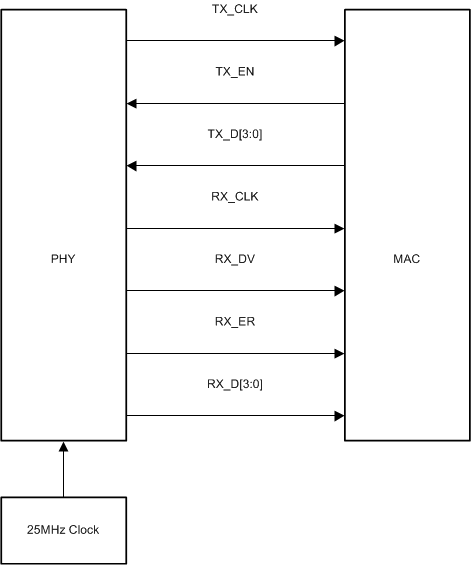
DP83869HM also supports MII mode when the PHY is working in 100M and 10M speeds. The user will have to ensure that the PHY links in either 100Mbps or 10Mbps mode. MII mode cannot be used in 1000Mbps mode. When using auto-negotiation to resolve MDI speed, TI recommends to turn off the gigabit speed advertisement through register 0x9 to ensure that the PHY does not link up at 1000Mbps speed. The Media Independent Interface is a synchronous 4-bit wide nibble data interface that connects the PHY to the MAC in 100BASE-FX, 100BASE-TX and 10BASE-Te modes. The RX_ER signal must be properly muxed by setting Register 18h to equal 0xE. The MII is fully compliant with IEEE 802.3-2002 clause 22.

The MII signals are summarized in Table 7-5:

Table 7-5 MII Signals
FUNCTIONPINS
Data SignalsTX_D[3:0]
RX_D[3:0]
Transmit and Receive SignalsTX_EN, TX_ER
RX_DV, RX_ER
DP83869HM MII SignalingFigure 7-8 MII Signaling
Note: MII mode cannot be enabled via straps alone. Register configuration is also needed.

Steps to configure DP83869HM to MII Mode:

  1. Write Reg 0x18 = 0xE
  2. Choose MDI Interface
    1. Copper:
      1. Write Reg 0x1DF = 0x60
    2. Fiber:
      1. Write Reg 0x1DF = 0x62
  3. Strap DP83869HM according to Table 7-6
Table 7-6 Strap Table for MII Mode
PIN NAME STRAP NAME PIN # PIN STRAP CONNECTION
JTAG_TDO / GPIO_1 OPMODE_0 22 OPEN
RX_D3 OPMODE_1 36

MII to Copper: OPEN

MII to Fiber: 2.49kΩ Pull-up to VDDIO

RX_D2 OPMODE_2 35 OPEN