SNLS654C April   2021  – November 2024 DP83TC812R-Q1 , DP83TC812S-Q1

PRODUCTION DATA  

  1.   1
  2. Features
  3. Applications
  4. Description
  5. Device Comparison Table
  6. Pin Configuration and Functions
  7. Specifications
    1. 6.1 Absolute Maximum Ratings
    2. 6.2 ESD Ratings
    3. 6.3 Recommended Operating Conditions
    4. 6.4 Thermal Information
    5. 6.5 Electrical Characteristics
    6. 6.6 Timing Requirements
    7. 6.7 Timing Diagrams
    8. 6.8 Typical Characteristics
  8. Detailed Description
    1. 7.1 Overview
    2. 7.2 Functional Block Diagram
    3. 7.3 Feature Description
      1. 7.3.1 Diagnostic Tool Kit
        1. 7.3.1.1 Signal Quality Indicator
        2. 7.3.1.2 Electrostatic Discharge Sensing
        3. 7.3.1.3 Time Domain Reflectometry
        4. 7.3.1.4 Voltage Sensing
        5. 7.3.1.5 BIST and Loopback Modes
          1. 7.3.1.5.1 Data Generator and Checker
          2. 7.3.1.5.2 xMII Loopback
          3. 7.3.1.5.3 PCS Loopback
          4. 7.3.1.5.4 Digital Loopback
          5. 7.3.1.5.5 Analog Loopback
          6. 7.3.1.5.6 Reverse Loopback
      2. 7.3.2 Compliance Test Modes
        1. 7.3.2.1 Test Mode 1
        2. 7.3.2.2 Test Mode 2
        3. 7.3.2.3 Test Mode 4
        4. 7.3.2.4 Test Mode 5
    4. 7.4 Device Functional Modes
      1. 7.4.1  Power Down
      2. 7.4.2  Reset
      3. 7.4.3  Standby
      4. 7.4.4  Normal
      5. 7.4.5  Sleep Ack
      6. 7.4.6  Sleep Request
      7. 7.4.7  Sleep Fail
      8. 7.4.8  Sleep
      9. 7.4.9  Wake-Up
      10. 7.4.10 TC10 System Example
      11. 7.4.11 Media Dependent Interface
        1. 7.4.11.1 100BASE-T1 Master and 100BASE-T1 Slave Configuration
        2. 7.4.11.2 Auto-Polarity Detection and Correction
        3. 7.4.11.3 Jabber Detection
        4. 7.4.11.4 Interleave Detection
      12. 7.4.12 MAC Interfaces
        1. 7.4.12.1 Media Independent Interface
        2. 7.4.12.2 Reduced Media Independent Interface
        3. 7.4.12.3 Reduced Gigabit Media Independent Interface
        4. 7.4.12.4 Serial Gigabit Media Independent Interface
      13. 7.4.13 Serial Management Interface
        1. 7.4.13.1 Direct Register Access
        2. 7.4.13.2 Extended Register Space Access
        3. 7.4.13.3 Write Operation (No Post Increment)
        4. 7.4.13.4 Read Operation (No Post Increment)
        5. 7.4.13.5 Write Operation (Post Increment)
        6. 7.4.13.6 Read Operation (Post Increment)
    5. 7.5 Programming
      1. 7.5.1 Strap Configuration
      2. 7.5.2 LED Configuration
      3. 7.5.3 PHY Address Configuration
    6. 7.6 Register Maps
      1. 7.6.1 Register Access Summary
      2. 7.6.2 DP83TC812 Registers
  9. Application and Implementation
    1. 8.1 Application Information Disclaimer
    2. 8.2 Application Information
    3. 8.3 Typical Applications
      1. 8.3.1 Design Requirements
        1. 8.3.1.1 Physical Medium Attachment
          1. 8.3.1.1.1 Common-Mode Choke Recommendations
      2. 8.3.2 Detailed Design Procedure
      3. 8.3.3 Application Curves
    4. 8.4 Power Supply Recommendations
    5. 8.5 Layout
      1. 8.5.1 Layout Guidelines
        1. 8.5.1.1 Signal Traces
        2. 8.5.1.2 Return Path
        3. 8.5.1.3 Metal Pour
        4. 8.5.1.4 PCB Layer Stacking
      2. 8.5.2 Layout Example
  10. Device and Documentation Support
    1. 9.1 Receiving Notification of Documentation Updates
    2. 9.2 Support Resources
    3. 9.3 Community Resources
    4. 9.4 Trademarks
    5. 9.5 Electrostatic Discharge Caution
    6. 9.6 Glossary
  11. 10Revision History
  12. 11Mechanical, Packaging, and Orderable Information

Package Options

Mechanical Data (Package|Pins)
Thermal pad, mechanical data (Package|Pins)
Orderable Information

PCB Layer Stacking

To meet signal integrity and performance requirements, minimum four-layer PCB is recommended. However, a six-layer PCB and above must be used when possible.
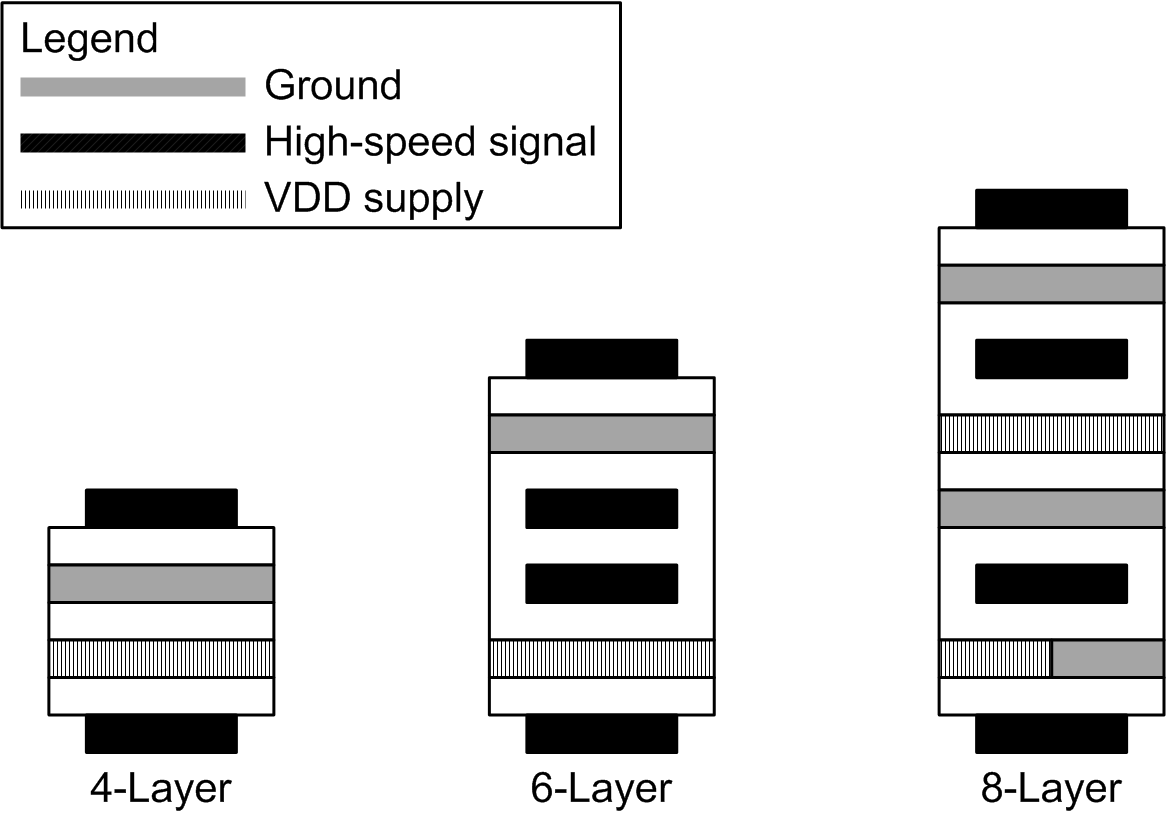
DP83TC812S-Q1 DP83TC812R-Q1 Recommended PCB
          Layer Stack-Up Figure 8-12 Recommended PCB Layer Stack-Up