SNLS654C April   2021  – November 2024 DP83TC812R-Q1 , DP83TC812S-Q1

PRODUCTION DATA  

  1.   1
  2. Features
  3. Applications
  4. Description
  5. Device Comparison Table
  6. Pin Configuration and Functions
  7. Specifications
    1. 6.1 Absolute Maximum Ratings
    2. 6.2 ESD Ratings
    3. 6.3 Recommended Operating Conditions
    4. 6.4 Thermal Information
    5. 6.5 Electrical Characteristics
    6. 6.6 Timing Requirements
    7. 6.7 Timing Diagrams
    8. 6.8 Typical Characteristics
  8. Detailed Description
    1. 7.1 Overview
    2. 7.2 Functional Block Diagram
    3. 7.3 Feature Description
      1. 7.3.1 Diagnostic Tool Kit
        1. 7.3.1.1 Signal Quality Indicator
        2. 7.3.1.2 Electrostatic Discharge Sensing
        3. 7.3.1.3 Time Domain Reflectometry
        4. 7.3.1.4 Voltage Sensing
        5. 7.3.1.5 BIST and Loopback Modes
          1. 7.3.1.5.1 Data Generator and Checker
          2. 7.3.1.5.2 xMII Loopback
          3. 7.3.1.5.3 PCS Loopback
          4. 7.3.1.5.4 Digital Loopback
          5. 7.3.1.5.5 Analog Loopback
          6. 7.3.1.5.6 Reverse Loopback
      2. 7.3.2 Compliance Test Modes
        1. 7.3.2.1 Test Mode 1
        2. 7.3.2.2 Test Mode 2
        3. 7.3.2.3 Test Mode 4
        4. 7.3.2.4 Test Mode 5
    4. 7.4 Device Functional Modes
      1. 7.4.1  Power Down
      2. 7.4.2  Reset
      3. 7.4.3  Standby
      4. 7.4.4  Normal
      5. 7.4.5  Sleep Ack
      6. 7.4.6  Sleep Request
      7. 7.4.7  Sleep Fail
      8. 7.4.8  Sleep
      9. 7.4.9  Wake-Up
      10. 7.4.10 TC10 System Example
      11. 7.4.11 Media Dependent Interface
        1. 7.4.11.1 100BASE-T1 Master and 100BASE-T1 Slave Configuration
        2. 7.4.11.2 Auto-Polarity Detection and Correction
        3. 7.4.11.3 Jabber Detection
        4. 7.4.11.4 Interleave Detection
      12. 7.4.12 MAC Interfaces
        1. 7.4.12.1 Media Independent Interface
        2. 7.4.12.2 Reduced Media Independent Interface
        3. 7.4.12.3 Reduced Gigabit Media Independent Interface
        4. 7.4.12.4 Serial Gigabit Media Independent Interface
      13. 7.4.13 Serial Management Interface
        1. 7.4.13.1 Direct Register Access
        2. 7.4.13.2 Extended Register Space Access
        3. 7.4.13.3 Write Operation (No Post Increment)
        4. 7.4.13.4 Read Operation (No Post Increment)
        5. 7.4.13.5 Write Operation (Post Increment)
        6. 7.4.13.6 Read Operation (Post Increment)
    5. 7.5 Programming
      1. 7.5.1 Strap Configuration
      2. 7.5.2 LED Configuration
      3. 7.5.3 PHY Address Configuration
    6. 7.6 Register Maps
      1. 7.6.1 Register Access Summary
      2. 7.6.2 DP83TC812 Registers
  9. Application and Implementation
    1. 8.1 Application Information Disclaimer
    2. 8.2 Application Information
    3. 8.3 Typical Applications
      1. 8.3.1 Design Requirements
        1. 8.3.1.1 Physical Medium Attachment
          1. 8.3.1.1.1 Common-Mode Choke Recommendations
      2. 8.3.2 Detailed Design Procedure
      3. 8.3.3 Application Curves
    4. 8.4 Power Supply Recommendations
    5. 8.5 Layout
      1. 8.5.1 Layout Guidelines
        1. 8.5.1.1 Signal Traces
        2. 8.5.1.2 Return Path
        3. 8.5.1.3 Metal Pour
        4. 8.5.1.4 PCB Layer Stacking
      2. 8.5.2 Layout Example
  10. Device and Documentation Support
    1. 9.1 Receiving Notification of Documentation Updates
    2. 9.2 Support Resources
    3. 9.3 Community Resources
    4. 9.4 Trademarks
    5. 9.5 Electrostatic Discharge Caution
    6. 9.6 Glossary
  11. 10Revision History
  12. 11Mechanical, Packaging, and Orderable Information

Package Options

Mechanical Data (Package|Pins)
Thermal pad, mechanical data (Package|Pins)
Orderable Information

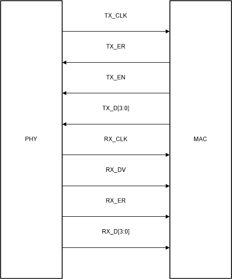
Media Independent Interface

The Media Independent Interface (MII) is a synchronous 4-bit wide nibble data interface that connects the PHY to the MAC. The MII is fully compliant with IEEE 802.3-2015 clause 22. The PHY has internal series termination resistors on MII output pins including TX_CLK output when the PHY is operating in MII mode. In this mode, it is recommended to not leave the MII-TX pins floating or High-Z.

The MII signals are summarized in Table 7-4:

Table 7-4 MII Signals
FUNCTIONPINS
Data SignalsTX_D[3:0]
RX_D[3:0]
Control SignalsTX_EN, TX_ER
RX_DV, RX_ER
Clock SignalsTX_CLK
RX_CLK
DP83TC812S-Q1 DP83TC812R-Q1 MII SignalingFigure 7-14 MII Signaling
Table 7-5 MII Transmit Encoding
TX_ENTX_ERTX_D[3:0]DESCRIPTION
000000 through 1111Normal Inter-Frame
010000 through 1111Reserved
100000 through 1111Normal Data Transmission
110000 through 1111Transmit Error Propagation
Table 7-6 MII Receive Encoding
RX_DVRX_ERRX_D[3:0]DESCRIPTION
000000 through 1111Normal Inter-Frame
010000Normal Inter-Frame
010001 through 1101Reserved
011110False Carrier Indication
011111Reserved
100000 through 1111Normal Data Reception
110000 through 1111Data Reception with Errors