SNLS654C April 2021 – November 2024 DP83TC812R-Q1 , DP83TC812S-Q1
PRODUCTION DATA
- 1
- 1 Features
- 2 Applications
- 3 Description
- 4 Device Comparison Table
- 5 Pin Configuration and Functions
- 6 Specifications
-
7 Detailed Description
- 7.1 Overview
- 7.2 Functional Block Diagram
- 7.3 Feature Description
- 7.4 Device Functional Modes
- 7.5 Programming
- 7.6 Register Maps
- 8 Application and Implementation
- 9 Device and Documentation Support
- 10Revision History
- 11Mechanical, Packaging, and Orderable Information
Package Options
Mechanical Data (Package|Pins)
- RHA|36
Thermal pad, mechanical data (Package|Pins)
- RHA|36
Orderable Information
7.4.12.2 Reduced Media Independent Interface
The DP83TC812-Q1 incorporates the Reduced Media Independent Interface (RMII) as defined in the RMII Revision 1.2 and 1.0 from the RMII consortium. The purpose of this interface is to provide a reduced pin count alternative to the IEEE 802.3u MII as specified in Clause 22. Architecturally, the RMII specification provides an additional reconciliation layer on either side of the MII, but can be implemented in the absence of an MII.
The DP83TC812-Q1 offers two types of RMII operations: RMII Slave and RMII Master. In RMII Slave Mode, the DP83TC812-Q1 operates off a 50MHz CMOS-level oscillator, which is either provided by the MAC or synchronous to the MAC's reference clock. In RMII Master operation, the DP83TC812-Q1 operates off of either a 25MHz CMOS-level oscillator connected to XI pin or a 25MHz crystal connected across XI and XO pins. When bootstrapping to RMII Master Mode, a 50MHz output clock will automatically be enabled on RX_D3. This 50MHz output clock must be routed to the MAC.
The RMII specification has the following characteristics:
- Single clock reference shared between MAC and PHY
- Provides independent 2-bit wide transmit and receive data paths
In this mode, data transfers are two bits for every clock cycle using the 50MHz reference clock for both transmit and receive paths.
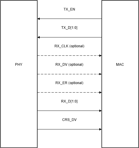
The RMII signals are summarized in Table 7-7:
| FUNCTION | PINS |
|---|---|
| Data Signals | TX_D[1:0] |
| RX_D[1:0] | |
| Control Signals | TX_EN |
| CRS_DV |
 Figure 7-15 RMII Signaling
| TX_EN | TX_D[1:0] | DESCRIPTION |
|---|---|---|
| 0 | 00 through 11 | Normal Inter-Frame |
| 1 | 00 through 11 | Normal Data Transmission |
| CRS_DV | RX_ER | RX_D[1:0] | DESCRIPTION |
|---|---|---|---|
| 0 | 0 | 00 through 11 | Normal Inter-Frame |
| 0 | 1 | 00 | Normal Inter-Frame |
| 0 | 1 | 01 through 11 | Reserved |
| 1 | 0 | 00 through 11 | Normal Data Reception |
| 1 | 1 | 00 through 11 | Data Reception with Errors |
RMII Slave: Data on TX_D[1:0] are latched at the PHY with reference to the rising edge of the reference clock at the XI pin. Data is presented on RX_D[1:0] with reference to the same rising clock edges at the XI pin.
RMII Master: Data on TX_D[1:0] are latched at the PHY with reference to the rising edge of the reference clock at the RX_D3 pin. Data is presented on RX_D[1:0] with reference to the same rising clock edges at the RX_D3 pin.
The DP83TC812-Q1 RMII supplies an RX_DV signal, which provides a simpler method to recover receive data without the need to separate RX_DV from the CRS_DV indication. RX_ER is also supported even though it is not required by the RMII specification.
RMII includes a programmable FIFO to adjust for the frequency differences between the reference clock and the recovered clock. The programmable FIFO, located in the register 0x0011[9:8] and register 0x0648[9:7], minimizes internal propagation delay based on expected maximum packet size and clock accuracy.
| Reg 0x0011 <9:8> | Reg 0x0648 <9:7> | Increment PHY latency | Max packet length without errors |
|---|---|---|---|
| 01 | 010 | Default | 2250 |
| 10 | 100 | 80 ns | 7250 |