SNLS676 May 2022 DP83TC813R-Q1 , DP83TC813S-Q1
PRODUCTION DATA
- 1 Features
- 2 Applications
- 3 Description
- 4 Revision History
- 5 Device Comparison Table
- 6 Pin Configuration and Functions
- 7 Specifications
-
8 Detailed Description
- 8.1 Overview
- 8.2 Functional Block Diagram
- 8.3 Feature Description
- 8.4
Device Functional Modes
- 8.4.1 Power Down
- 8.4.2 Reset
- 8.4.3 Standby
- 8.4.4 Normal
- 8.4.5 Sleep Ack
- 8.4.6 Sleep Request
- 8.4.7 Sleep Fail
- 8.4.8 Sleep
- 8.4.9 Wake-Up
- 8.4.10 TC10 System Example
- 8.4.11 Media Dependent Interface
- 8.4.12 MAC Interfaces
- 8.4.13 Serial Management Interface
- 8.4.14 Direct Register Access
- 8.4.15 Extended Register Space Access
- 8.4.16 Write Address Operation
- 8.4.17 Read Address Operation
- 8.4.18 Write Operation (No Post Increment)
- 8.4.19 Read Operation (No Post Increment)
- 8.4.20 Write Operation (Post Increment)
- 8.4.21 Read Operation (Post Increment)
- 8.5 Programming
- 8.6 Register Maps
- 9 Application and Implementation
- 10Power Supply Recommendations
- 11Layout
- 12Device and Documentation Support
- 13Mechanical, Packaging, and Orderable Information
Package Options
Mechanical Data (Package|Pins)
- RHF|28
Thermal pad, mechanical data (Package|Pins)
- RHF|28
Orderable Information
7.7 Timing Diagrams
Figure 7-1 MII
Timing
Figure 7-2 RMII Transmit and
Receive Timing
Figure 7-3 RGMII Transmit
Timing (Internal Delay Enabled)
 Figure 7-4 RGMII Transmit Timing (Internal Delay Disabled)
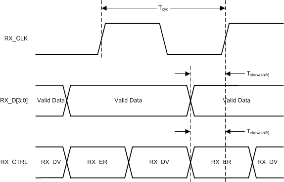
 Figure 7-5 RGMII Receive Timing (Internal Delay Enabled)
 Figure 7-6 RGMII Receive Timing (Internal Delay Disabled)
 Figure 7-7 Serial Management Timing
Figure 7-8 Power-Up
Timing
Figure 7-9 Reset
Timing
Figure 7-10 WAKE Timing