SNLS656D August 2020 – December 2023 DP83TD510E
PRODUCTION DATA
- 1
- 1 Features
- 2 Applications
- 3 Description
- 4 Pin Configuration and Functions
- 5 Specifications
-
6 Detailed Description
- 6.1 Overview
- 6.2 Functional Block Diagram
- 6.3
Feature Description
- 6.3.1 Auto-Negotiation (Speed Selection)
- 6.3.2 Repeater Mode
- 6.3.3 Media Converter
- 6.3.4 Clock Output
- 6.3.5 Media Independent Interface (MII)
- 6.3.6 Reduced Media Independent Interface (RMII)
- 6.3.7 RMII Low Power 5-MHz Mode
- 6.3.8 RGMII Interface
- 6.3.9 Serial Management Interface
- 6.3.10 Extended Register Space Access
- 6.3.11 Loopback Modes
- 6.3.12 BIST Configurations
- 6.3.13 Cable Diagnostics
- 6.4 Device Functional Modes
- 6.5 Programming
- 6.6 MMD Register Address Map
- 6.7 DP83TD510E Registers
- 7 Application and Implementation
- 8 Device and Documentation Support
- 9 Revision History
- 10Mechanical, Packaging, and Orderable Information
Package Options
Mechanical Data (Package|Pins)
- RHB|32
Thermal pad, mechanical data (Package|Pins)
- RHB|32
Orderable Information
7.3 Power Supply Recommendations
The DP83TD510E is capable of operating from Single Supply 3V3. It supports single supply operations from 1V8 for Short Reach ( 1v p2p) mode. It also supports Dual Supply Operations for Lowest Power Dissipation. It also supports VDDIO to work at 3.3-V, 2.5-V or 1.8-V supply voltages PHY has capability to detect the power supply levels automatically for both AVDD and VDDIO..
Single Power Supply Operations : Analog supply shall be powered by 3.3 V or 1.8 V. AVDD of 3V3 can support both Long Reach ( 2.4-v p2p) and Short Reach( 1-v p2p).
Please note with AVDD 1.8 V, only Short Cable mode of 1-V p2p will be supported.
Appropriate straps shall be configured to ensure Auto Negotiation transmits the correct capabilities of the PHY.
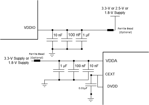
The recommended power supply de-coupling network is shown below:
 Figure 7-5 DP83TD510E Single Power Supply Decoupling Recommendation
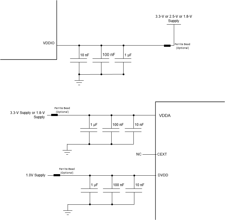
For Dual Supply Operations, digital voltage rail of 1.0 V externally shall be supplied seperately. This help reduce the power consumption further of the DP83TD510E. See below connections for Dual Power Supply.
 Figure 7-6 DP83TD510E Dual Supply
Power Supply Decoupling Recommendation