SNLS656D August 2020 – December 2023 DP83TD510E
PRODUCTION DATA
- 1
- 1 Features
- 2 Applications
- 3 Description
- 4 Pin Configuration and Functions
- 5 Specifications
-
6 Detailed Description
- 6.1 Overview
- 6.2 Functional Block Diagram
- 6.3
Feature Description
- 6.3.1 Auto-Negotiation (Speed Selection)
- 6.3.2 Repeater Mode
- 6.3.3 Media Converter
- 6.3.4 Clock Output
- 6.3.5 Media Independent Interface (MII)
- 6.3.6 Reduced Media Independent Interface (RMII)
- 6.3.7 RMII Low Power 5-MHz Mode
- 6.3.8 RGMII Interface
- 6.3.9 Serial Management Interface
- 6.3.10 Extended Register Space Access
- 6.3.11 Loopback Modes
- 6.3.12 BIST Configurations
- 6.3.13 Cable Diagnostics
- 6.4 Device Functional Modes
- 6.5 Programming
- 6.6 MMD Register Address Map
- 6.7 DP83TD510E Registers
- 7 Application and Implementation
- 8 Device and Documentation Support
- 9 Revision History
- 10Mechanical, Packaging, and Orderable Information
Package Options
Mechanical Data (Package|Pins)
- RHB|32
Thermal pad, mechanical data (Package|Pins)
- RHB|32
Orderable Information
6.3.6 Reduced Media Independent Interface (RMII)
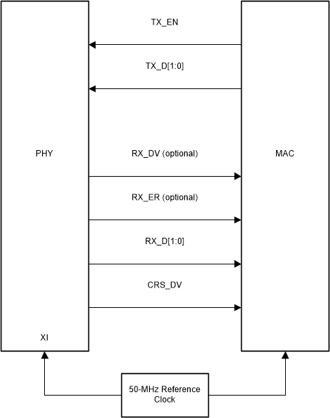
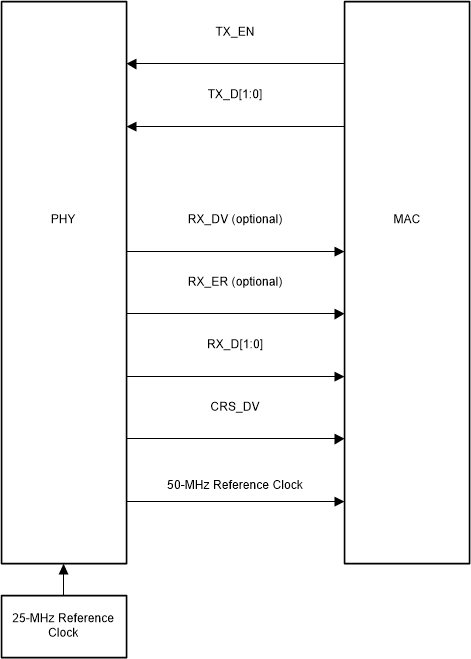
The DP83TD510E incorporates the Reduced Media Independent Interface (RMII) as specified in the RMII specification v1.2. The purpose of this interface is to provide a reduced pin count alternative to the IEEE 802.3 MII as specified in Clause 22. Architecturally, the RMII specification provides an additional reconciliation layer on either side of the MII, but can be implemented in the absence of an MII. The DP83TD510E offers two types of RMII operations: RMII Slave and RMII Master. In RMII Master operation, the DP83TD510E operates off of either a 25-MHz CMOS-level oscillator connected to XI pin or a 25-MHz crystal connected across XI and XO pins. A 50-MHz output clock referenced from DP83TD510E can be connected to the MAC. In RMII Slave operation, the DP83TD510E operates off of a 50-MHz CMOS-level oscillator connected to the XI pin and shares the same clock as the MAC. Alternatively, in RMII Slave mode, the PHY can run from a 50-MHz clock provided by the Host MAC.
The RMII specification has the following characteristics:
- Single clock reference sourced from the PHY to MAC or from an external source fed both to MAC and PHY
- Independent 2-bit wide transmit and receive data paths
- Usage of CMOS signal levels, the same levels as the MII interface
In this mode, data transfers are two bits for every clock cycle using the internal 50-MHz reference clock for both transmit and receive paths.
The RMII signals are summarized in Table 6-2.
| FUNCTION | PINS |
|---|---|
| Receive Data Lines | TX_D[1:0] |
| Transmit Data Lines | RX_D[1:0] |
| Receive Control Signal | TX_EN |
| Transmit Control Signal | CRS_DV |
 Figure 6-5 RMII Slave Signaling
 Figure 6-6 RMII Master Signaling
Data on TX_D[1:0] are latched at the PHY with reference to the clock edges on the XI pin. Data on RX_D[1:0] are latched at the MAC with reference to the same clock edges on the XI pin in RMII Slave Mode. For RMII Master mode, data is latched wrt the CLKOUT50M output from the PHY.
In addition, CRX_DV can be configured as RX_DV signal. It allows a simpler method of recovering receive data without the need to separate RX_DV from the CRS_DV indication.