SPRS956H March 2016 – November 2019 DRA722 , DRA724 , DRA725 , DRA726
PRODUCTION DATA.
- 1 Device Overview
- 2 Revision History
- 3 Device Comparison
-
4 Terminal Configuration and Functions
- 4.1 Terminal Assignment
- 4.2 Ball Characteristics
- 4.3 Multiplexing Characteristics
- 4.4
Signal Descriptions
- 4.4.1 Video Input Ports (VIP)
- 4.4.2 Display Subsystem – Video Output Ports
- 4.4.3 Display Subsystem – High-Definition Multimedia Interface (HDMI)
- 4.4.4 Camera Serial Interface 2 CAL bridge (CSI2)
- 4.4.5 External Memory Interface (EMIF)
- 4.4.6 General-Purpose Memory Controller (GPMC)
- 4.4.7 Timers
- 4.4.8 Inter-Integrated Circuit Interface (I2C)
- 4.4.9 HDQ / 1-Wire Interface (HDQ1W)
- 4.4.10 Universal Asynchronous Receiver Transmitter (UART)
- 4.4.11 Multichannel Serial Peripheral Interface (McSPI)
- 4.4.12 Quad Serial Peripheral Interface (QSPI)
- 4.4.13 Multicannel Audio Serial Port (McASP)
- 4.4.14 Universal Serial Bus (USB)
- 4.4.15 SATA
- 4.4.16 Peripheral Component Interconnect Express (PCIe)
- 4.4.17 Controller Area Network Interface (DCAN)
- 4.4.18 Ethernet Interface (GMAC_SW)
- 4.4.19 Media Local Bus (MLB) Interface
- 4.4.20 eMMC/SD/SDIO
- 4.4.21 General-Purpose Interface (GPIO)
- 4.4.22 Keyboard controller (KBD)
- 4.4.23 Pulse Width Modulation (PWM) Interface
- 4.4.24 Audio Tracking Logic (ATL)
- 4.4.25 Test Interfaces
- 4.4.26 System and Miscellaneous
- 4.4.27 Power Supplies
-
5 Specifications
- 5.1 Absolute Maximum Ratings
- 5.2 ESD Ratings
- 5.3 Power-On-Hour (POH) Limits
- 5.4 Recommended Operating Conditions
- 5.5 Operating Performance Points
- 5.6 Power Consumption Summary
- 5.7
Electrical Characteristics
- 5.7.1 LVCMOS DDR DC Electrical Characteristics
- 5.7.2 HDMIPHY DC Electrical Characteristics
- 5.7.3 Dual Voltage LVCMOS I2C DC Electrical Characteristics
- 5.7.4 IQ1833 Buffers DC Electrical Characteristics
- 5.7.5 IHHV1833 Buffers DC Electrical Characteristics
- 5.7.6 LVCMOS OSC Buffers DC Electrical Characteristics
- 5.7.7 LVCMOS CSI2 DC Electrical Characteristics
- 5.7.8 BMLB18 Buffers DC Electrical Characteristics
- 5.7.9 BC1833IHHV Buffers DC Electrical Characteristics
- 5.7.10 USBPHY DC Electrical Characteristics
- 5.7.11 Dual Voltage SDIO1833 DC Electrical Characteristics
- 5.7.12 Dual Voltage LVCMOS DC Electrical Characteristics
- 5.7.13 SATAPHY DC Electrical Characteristics
- 5.7.14 PCIEPHY DC Electrical Characteristics
- 5.8 VPP Specifications for One-Time Programmable (OTP) eFuses
- 5.9 Thermal Characteristics
- 5.10 Power Supply Sequences
- 6 Clock Specifications
-
7 Timing Requirements and Switching Characteristics
- 7.1 Timing Test Conditions
- 7.2 Interface Clock Specifications
- 7.3 Timing Parameters and Information
- 7.4 Recommended Clock and Control Signal Transition Behavior
- 7.5 Virtual and Manual I/O Timing Modes
- 7.6 Video Input Ports (VIP)
- 7.7 Display Subsystem - Video Output Ports
- 7.8 Display Subsystem - High-Definition Multimedia Interface (HDMI)
- 7.9 Camera Serial Interface 2 CAL bridge (CSI2)
- 7.10 External Memory Interface (EMIF)
- 7.11 General-Purpose Memory Controller (GPMC)
- 7.12 Timers
- 7.13 Inter-Integrated Circuit Interface (I2C)
- 7.14 HDQ / 1-Wire Interface (HDQ1W)
- 7.15 Universal Asynchronous Receiver Transmitter (UART)
- 7.16 Multichannel Serial Peripheral Interface (McSPI)
- 7.17 Quad Serial Peripheral Interface (QSPI)
- 7.18 Multichannel Audio Serial Port (McASP)
- 7.19 Universal Serial Bus (USB)
- 7.20 Serial Advanced Technology Attachment (SATA)
- 7.21 Peripheral Component Interconnect Express (PCIe)
- 7.22 Controller Area Network Interface (DCAN)
- 7.23
Ethernet Interface (GMAC_SW)
- 7.23.1
GMAC MII Timings
- Table 7-70 Timing Requirements for miin_rxclk - MII Operation
- Table 7-71 Timing Requirements for miin_txclk - MII Operation
- Table 7-72 Timing Requirements for GMAC MIIn Receive 10/100 Mbit/s
- Table 7-73 Switching Characteristics Over Recommended Operating Conditions for GMAC MIIn Transmit 10/100 Mbits/s
- 7.23.2 GMAC MDIO Interface Timings
- 7.23.3
GMAC RMII Timings
- Table 7-78 Timing Requirements for GMAC REF_CLK - RMII Operation
- Table 7-79 Timing Requirements for GMAC RMIIn Receive
- Table 7-80 Switching Characteristics Over Recommended Operating Conditions for GMAC REF_CLK - RMII Operation
- Table 7-81 Switching Characteristics Over Recommended Operating Conditions for GMAC RMIIn Transmit 10/100 Mbits/s
- 7.23.4
GMAC RGMII Timings
- Table 7-85 Timing Requirements for rgmiin_rxc - RGMIIn Operation
- Table 7-86 Timing Requirements for GMAC RGMIIn Input Receive for 10/100/1000 Mbps
- Table 7-87 Switching Characteristics Over Recommended Operating Conditions for rgmiin_txctl - RGMIIn Operation for 10/100/1000 Mbit/s
- Table 7-88 Switching Characteristics for GMAC RGMIIn Output Transmit for 10/100/1000 Mbps
- 7.23.1
GMAC MII Timings
- 7.24 Media Local Bus (MLB) interface
- 7.25
eMMC/SD/SDIO
- 7.25.1
MMC1-SD Card Interface
- 7.25.1.1 Default speed, 4-bit data, SDR, half-cycle
- 7.25.1.2 High speed, 4-bit data, SDR, half-cycle
- 7.25.1.3 SDR12, 4-bit data, half-cycle
- 7.25.1.4 SDR25, 4-bit data, half-cycle
- 7.25.1.5 UHS-I SDR50, 4-bit data, half-cycle
- 7.25.1.6 UHS-I SDR104, 4-bit data, half-cycle
- 7.25.1.7 UHS-I DDR50, 4-bit data
- 7.25.2 MMC2 - eMMC
- 7.25.3 MMC3 and MMC4-SDIO/SD
- 7.25.1
MMC1-SD Card Interface
- 7.26 General-Purpose Interface (GPIO)
- 7.27 Audio Tracking Logic (ATL)
- 7.28 System and Miscellaneous interfaces
- 7.29
Test Interfaces
- 7.29.1
IEEE 1149.1 Standard-Test-Access Port (JTAG)
- 7.29.1.1
JTAG Electrical Data/Timing
- Table 7-142 Timing Requirements for IEEE 1149.1 JTAG
- Table 7-143 Switching Characteristics Over Recommended Operating Conditions for IEEE 1149.1 JTAG
- Table 7-144 Timing Requirements for IEEE 1149.1 JTAG With RTCK
- Table 7-145 Switching Characteristics Over Recommended Operating Conditions for IEEE 1149.1 JTAG With RTCK
- 7.29.1.1
JTAG Electrical Data/Timing
- 7.29.2 Trace Port Interface Unit (TPIU)
- 7.29.1
IEEE 1149.1 Standard-Test-Access Port (JTAG)
-
8 Applications, Implementation, and Layout
- 8.1 Introduction
- 8.2 Power Optimizations
- 8.3 Core Power Domains
- 8.4 Single-Ended Interfaces
- 8.5
Differential Interfaces
- 8.5.1 General Routing Guidelines
- 8.5.2
USB 2.0 Board Design and Layout Guidelines
- 8.5.2.1 Background
- 8.5.2.2
USB PHY Layout Guide
- 8.5.2.2.1 General Routing and Placement
- 8.5.2.2.2
Specific Guidelines for USB PHY Layout
- 8.5.2.2.2.1 Analog, PLL, and Digital Power Supply Filtering
- 8.5.2.2.2.2 Analog, Digital, and PLL Partitioning
- 8.5.2.2.2.3 Board Stackup
- 8.5.2.2.2.4 Cable Connector Socket
- 8.5.2.2.2.5 Clock Routings
- 8.5.2.2.2.6 Crystals/Oscillator
- 8.5.2.2.2.7 DP/DM Trace
- 8.5.2.2.2.8 DP/DM Vias
- 8.5.2.2.2.9 Image Planes
- 8.5.2.2.2.10 Power Regulators
- 8.5.2.3 References
- 8.5.3 USB 3.0 Board Design and Layout Guidelines
- 8.5.4 HDMI Board Design and Layout Guidelines
- 8.5.5 SATA Board Design and Layout Guidelines
- 8.5.6 PCIe Board Design and Layout Guidelines
- 8.5.7 CSI2 Board Design and Routing Guidelines
- 8.6 Clock Routing Guidelines
- 8.7
DDR3 Board Design and Layout Guidelines
- 8.7.1 DDR3 General Board Layout Guidelines
- 8.7.2
DDR3 Board Design and Layout Guidelines
- 8.7.2.1 Board Designs
- 8.7.2.2 DDR3 EMIF
- 8.7.2.3 DDR3 Device Combinations
- 8.7.2.4 DDR3 Interface Schematic
- 8.7.2.5 Compatible JEDEC DDR3 Devices
- 8.7.2.6 PCB Stackup
- 8.7.2.7 Placement
- 8.7.2.8 DDR3 Keepout Region
- 8.7.2.9 Bulk Bypass Capacitors
- 8.7.2.10 High Speed Bypass Capacitors
- 8.7.2.11 Net Classes
- 8.7.2.12 DDR3 Signal Termination
- 8.7.2.13 VREF_DDR Routing
- 8.7.2.14 VTT
- 8.7.2.15 CK and ADDR_CTRL Topologies and Routing Definition
- 8.7.2.16 Data Topologies and Routing Definition
- 8.7.2.17 Routing Specification
- 9 Device and Documentation Support
- 10Mechanical, Packaging, and Orderable Information
Package Options
Refer to the PDF data sheet for device specific package drawings
Mechanical Data (Package|Pins)
- ABC|760
Thermal pad, mechanical data (Package|Pins)
Orderable Information
8.5.2.2.2.9 Image Planes
An image plane is a layer of copper (voltage plane or ground plane), physically adjacent to a signal routing plane. Use of image planes provides a low impedance, shortest possible return path for RF currents. For a USB board, the best image plane is the ground plane because it can be used for both analog and digital circuits.
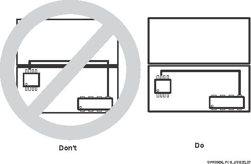
- Do not route traces so they cross from one plane to the other. This can cause a broken RF return path resulting in an EMI radiating loop as shown in Figure 8-27. This is important for higher frequency or repetitive signals. Therefore, on a multi-layer board, it is best to run all clock signals on the signal plane above a solid ground plane.
- Avoid crossing the image power or ground plane boundaries with high speed clock signal traces immediately above or below the separated planes. This also holds true for the twisted pair signals (DP, DM). Any unused area of the top and bottom signal layers of the PCB can be filled with copper that is connected to the ground plane through vias.
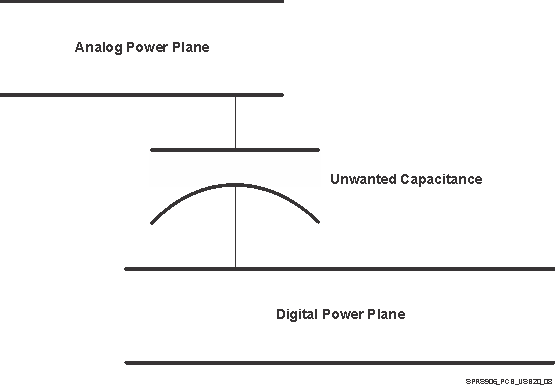
- Do not overlap planes that do not reference each other. For example, do not overlap a digital power plane with an analog power plane as this produces a capacitance between the overlapping areas that could pass RF emissions from one plane to the other, as shown in Figure 8-28.
- Avoid image plane violations. Traces that route over a slot in an image plane results in a possible RF return loop, as shown in Figure 8-29.
 Figure 8-27 Do Not Cross Plane Boundaries
  Figure 8-28 Do Not Overlap Planes
  Figure 8-29 Do Not Violate Image Planes