SPRS993E March 2017 – December 2018 DRA76P , DRA77P
PRODUCTION DATA.
- 1Device Overview
- 2Revision History
- 3Device Comparison
-
4Terminal Configuration and Functions
- 4.1 Pin Diagram
- 4.2 Pin Attributes
- 4.3
Signal Descriptions
- 4.3.1 VIP
- 4.3.2 DSS
- 4.3.3 HDMI
- 4.3.4 Camera Serial Interface 2 CAL bridge (CSI2)
- 4.3.5 EMIF
- 4.3.6 GPMC
- 4.3.7 Timers
- 4.3.8 I2C
- 4.3.9 HDQ1W
- 4.3.10 UART
- 4.3.11 McSPI
- 4.3.12 QSPI
- 4.3.13 McASP
- 4.3.14 USB
- 4.3.15 SATA
- 4.3.16 PCIe
- 4.3.17 DCAN and MCAN
- 4.3.18 GMAC_SW
- 4.3.19 MLB
- 4.3.20 eMMC/SD/SDIO
- 4.3.21 GPIO
- 4.3.22 KBD
- 4.3.23 PWM
- 4.3.24 ATL
- 4.3.25 Test Interfaces
- 4.3.26 System and Miscellaneous
- 4.4 Pin Multiplexing
- 4.5 Connections for Unused Pins
-
5Specifications
- 5.1 Absolute Maximum Ratings
- 5.2 ESD Ratings
- 5.3 Power-On Hours (POH)
- 5.4 Recommended Operating Conditions
- 5.5 Operating Performance Points
- 5.6 Power Consumption Summary
- 5.7
Electrical Characteristics
- Table 5-6 LVCMOS DDR DC Electrical Characteristics
- Table 5-7 Dual Voltage LVCMOS I2C DC Electrical Characteristics
- Table 5-8 IQ1833 Buffers DC Electrical Characteristics
- Table 5-9 LVCMOS CSI2 DC Electrical Characteristics
- Table 5-10 IHHV1833 Buffers DC Electrical Characteristics
- Table 5-11 BMLB18 Buffers DC Electrical Characteristics
- Table 5-12 Dual Voltage SDIO1833 DC Electrical Characteristics
- Table 5-13 Dual Voltage LVCMOS DC Electrical Characteristics
- 5.7.1 HDMIPHY DC Electrical Characteristics
- 5.7.2 USBPHY DC Electrical Characteristics
- 5.7.3 SATAPHY DC Electrical Characteristics
- 5.7.4 PCIEPHY DC Electrical Characteristics
- 5.8 VPP Specifications for One-Time Programmable (OTP) eFuses
- 5.9 Thermal Resistance Characteristics
- 5.10
Timing Requirements and Switching Characteristics
- 5.10.1 Timing Parameters and Information
- 5.10.2 Interface Clock Specifications
- 5.10.3 Power Supply Sequences
- 5.10.4 Clock Specifications
- 5.10.5 Recommended Clock and Control Signal Transition Behavior
- 5.10.6
Peripherals
- 5.10.6.1 Timing Test Conditions
- 5.10.6.2 Virtual and Manual I/O Timing Modes
- 5.10.6.3 VIP
- 5.10.6.4 DSS
- 5.10.6.5 HDMI
- 5.10.6.6 EMIF
- 5.10.6.7 GPMC
- 5.10.6.8 Timers
- 5.10.6.9 I2C
- 5.10.6.10 HDQ1W
- 5.10.6.11 UART
- 5.10.6.12 McSPI
- 5.10.6.13 QSPI
- 5.10.6.14
McASP
- Table 5-75 Timing Requirements for McASP1
- Table 5-76 Timing Requirements for McASP2
- Table 5-77 Timing Requirements for McASP3/4/5/6/7/8
- Table 5-78 Switching Characteristics Over Recommended Operating Conditions for McASP1
- Table 5-79 Switching Characteristics Over Recommended Operating Conditions for McASP2
- Table 5-80 Switching Characteristics Over Recommended Operating Conditions for McASP3/4/5/6/7/8
- 5.10.6.15 USB
- 5.10.6.16 SATA
- 5.10.6.17 PCIe
- 5.10.6.18 CAN
- 5.10.6.19
GMAC_SW
- 5.10.6.19.1
GMAC MII Timings
- Table 5-97 Timing Requirements for miin_rxclk - MII Operation
- Table 5-98 Timing Requirements for miin_txclk - MII Operation
- Table 5-99 Timing Requirements for GMAC MIIn Receive 10/100 Mbit/s
- Table 5-100 Switching Characteristics Over Recommended Operating Conditions for GMAC MIIn Transmit 10/100 Mbits/s
- 5.10.6.19.2 GMAC MDIO Interface Timings
- 5.10.6.19.3
GMAC RMII Timings
- Table 5-105 Timing Requirements for GMAC REF_CLK - RMII Operation
- Table 5-106 Timing Requirements for GMAC RMIIn Receive
- Table 5-107 Switching Characteristics Over Recommended Operating Conditions for GMAC REF_CLK - RMII Operation
- Table 5-108 Switching Characteristics Over Recommended Operating Conditions for GMAC RMIIn Transmit 10/100 Mbits/s
- 5.10.6.19.4
GMAC RGMII Timings
- Table 5-112 Timing Requirements for rgmiin_rxc - RGMIIn Operation
- Table 5-113 Timing Requirements for GMAC RGMIIn Input Receive for 10/100/1000 Mbps
- Table 5-114 Switching Characteristics Over Recommended Operating Conditions for rgmiin_txctl - RGMIIn Operation for 10/100/1000 Mbit/s
- Table 5-115 Switching Characteristics for GMAC RGMIIn Output Transmit for 10/100/1000 Mbps
- 5.10.6.19.1
GMAC MII Timings
- 5.10.6.20 MLB
- 5.10.6.21
eMMC/SD/SDIO
- 5.10.6.21.1
MMC1—SD Card Interface
- 5.10.6.21.1.1 Default speed, 4-bit Data, SDR, Half-Cycle
- 5.10.6.21.1.2 High-Speed, 4-bit Data, SDR, Half-Cycle
- 5.10.6.21.1.3 SDR12, 4-bit Data, Half-Cycle
- 5.10.6.21.1.4 SDR25, 4-bit Data, Half-Cycle
- 5.10.6.21.1.5 UHS-I SDR50, 4-bit Data, Half-Cycle
- 5.10.6.21.1.6 UHS-I SDR104, 4-bit Data, Half-Cycle
- 5.10.6.21.1.7 UHS-I DDR50, 4-bit Data
- 5.10.6.21.2 MMC2 — eMMC
- 5.10.6.21.3 MMC3 and MMC4—SDIO/SD
- 5.10.6.21.1
MMC1—SD Card Interface
- 5.10.6.22 GPIO
- 5.10.6.23 ATL
- 5.10.6.24 System and Miscellaneous Interfaces
- 5.10.7
Emulation and Debug Subsystem
- 5.10.7.1
JTAG
- 5.10.7.1.1
JTAG Electrical Data/Timing
- Table 5-172 Timing Requirements for IEEE 1149.1 JTAG
- Table 5-173 Switching Characteristics Over Recommended Operating Conditions for IEEE 1149.1 JTAG
- Table 5-174 Timing Requirements for IEEE 1149.1 JTAG With RTCK
- Table 5-175 Switching Characteristics Over Recommended Operating Conditions for IEEE 1149.1 JTAG With RTCK
- 5.10.7.1.1
JTAG Electrical Data/Timing
- 5.10.7.2 TPIU
- 5.10.7.1
JTAG
-
6Detailed Description
- 6.1 Description
- 6.2 Functional Block Diagram
- 6.3 MPU
- 6.4 DSP Subsystem
- 6.5 ISS
- 6.6 IVA
- 6.7 EVE
- 6.8 IPU
- 6.9 VPE
- 6.10 GPU
- 6.11 ATL Overview
- 6.12 Memory Subsystem
- 6.13 Interprocessor Communication
- 6.14 Interrupt Controller
- 6.15 EDMA
- 6.16 Peripherals
- 6.17 On-Chip Debug
-
7Applications, Implementation, and Layout
- 7.1 Introduction
- 7.2 Power Optimizations
- 7.3 Core Power Domains
- 7.4 Single-Ended Interfaces
- 7.5
Differential Interfaces
- 7.5.1 General Routing Guidelines
- 7.5.2
USB 2.0 Board Design and Layout Guidelines
- 7.5.2.1 Background
- 7.5.2.2
USB PHY Layout Guide
- 7.5.2.2.1 General Routing and Placement
- 7.5.2.2.2
Specific Guidelines for USB PHY Layout
- 7.5.2.2.2.1 Analog, PLL, and Digital Power Supply Filtering
- 7.5.2.2.2.2 Analog, Digital, and PLL Partitioning
- 7.5.2.2.2.3 Board Stackup
- 7.5.2.2.2.4 Cable Connector Socket
- 7.5.2.2.2.5 Clock Routings
- 7.5.2.2.2.6 Crystals/Oscillator
- 7.5.2.2.2.7 DP/DM Trace
- 7.5.2.2.2.8 DP/DM Vias
- 7.5.2.2.2.9 Image Planes
- 7.5.2.2.2.10 JTAG Interface
- 7.5.2.2.2.11 Power Regulators
- 7.5.2.3 Electrostatic Discharge (ESD)
- 7.5.2.4 References
- 7.5.3 USB 3.0 Board Design and Layout Guidelines
- 7.5.4 HDMI Board Design and Layout Guidelines
- 7.5.5 SATA Board Design and Layout Guidelines
- 7.5.6 PCIe Board Design and Layout Guidelines
- 7.5.7 CSI2 Board Design and Routing Guidelines
- 7.6
DDR2/DDR3 Board Design and Layout Guidelines
- 7.6.1 DDR2/DDR3 General Board Layout Guidelines
- 7.6.2 DDR2 Board Design and Layout Guidelines
- 7.6.3
DDR3 Board Design and Layout Guidelines
- 7.6.3.1 Board Designs
- 7.6.3.2 DDR3 EMIF
- 7.6.3.3 DDR3 Device Combinations
- 7.6.3.4 DDR3 Interface Schematic
- 7.6.3.5 Compatible JEDEC DDR3 Devices
- 7.6.3.6 PCB Stackup
- 7.6.3.7 Placement
- 7.6.3.8 DDR3 Keepout Region
- 7.6.3.9 Bulk Bypass Capacitors
- 7.6.3.10 High-Speed Bypass Capacitors
- 7.6.3.11 Net Classes
- 7.6.3.12 DDR3 Signal Termination
- 7.6.3.13 VREF_DDR Routing
- 7.6.3.14 VTT
- 7.6.3.15 CK and ADDR_CTRL Topologies and Routing Definition
- 7.6.3.16 Data Topologies and Routing Definition
- 7.6.3.17 Routing Specification
- 8Device and Documentation Support
- 9Mechanical Packaging and Orderable Information
Package Options
Refer to the PDF data sheet for device specific package drawings
Mechanical Data (Package|Pins)
- ACD|784
Thermal pad, mechanical data (Package|Pins)
Orderable Information
7.3.8.2 vdd_mpu Example Analysis
Maximum acceptable PCB resistance (Reff) between the PMIC and Processor input power balls should not exceed 10 mΩ.
Maximum decoupling capacitance loop inductance (LL) between Processor input power balls and decoupling capacitances should not exceed 2.0 nH (ESL NOT included)
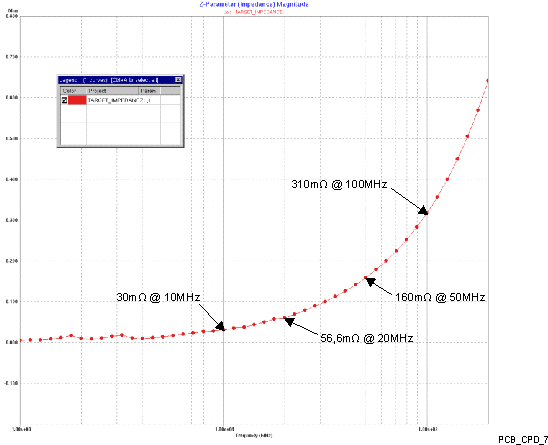
Impedance target for key frequency of interest between Processor input power balls and PMIC’s SMPS output power balls should not exceed 57 mΩ at 20 MHz.
Table 7-5 Example PCB vdd_mpu PI Analysis Summary
| Parameter | Recommendation | Example PCB |
|---|---|---|
| Processor OPP | High | |
| Clocking Rate | 1.5 GHz | |
| Voltage Level | 1.22 V | 1.22 V |
| Max Current Draw | 5.12 A | 5.12 A |
| Max Effective Resistance: Power Inductor Segment Total Reff | 10 mΩ | 9.0 mΩ |
| Max Loop Inductance | 2.0 nH | 1.0 – 1.4 nH |
| Impedance Target | 57 mΩ F < 20 MHz | 57 mΩ F < 20 MHz |
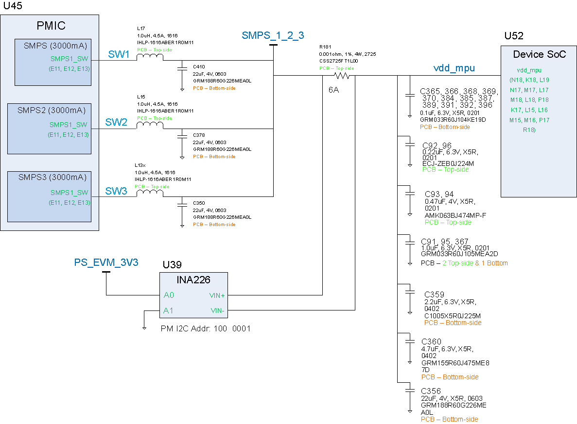
Figure 7-21, Figure 7-22, Figure 7-23, and Figure 7-24 show a PCB layout example and the resulting PI analysis results.
 Figure 7-21 vdd_mpu Simplified SCH Diagram
 ![DRA77P DRA76P vdd_mpu routing [Top Layer] DRA77P DRA76P VAYU_PCB_CPD_2.gif](/ods/images/SPRS993E/VAYU_PCB_CPD_2.gif) Figure 7-22 vdd_mpu routing [Top Layer]
Figure 7-22 vdd_mpu routing [Top Layer] ![DRA77P DRA76P vdd_mpu routing [Internal Power Plane #2] DRA77P DRA76P VAYU_PCB_CPD_3.gif](/ods/images/SPRS993E/VAYU_PCB_CPD_3.gif) Figure 7-23 vdd_mpu routing [Internal Power Plane #2]
Figure 7-23 vdd_mpu routing [Internal Power Plane #2] ![DRA77P DRA76P vdd_mpu routing and cap placements [Bottom Layer] DRA77P DRA76P VAYU_PCB_CPD_4.gif](/ods/images/SPRS993E/VAYU_PCB_CPD_4.gif) Figure 7-24 vdd_mpu routing and cap placements [Bottom Layer]
Figure 7-24 vdd_mpu routing and cap placements [Bottom Layer] Table 7-6 PCB Etch Resistance Breakdown - From PMIC Source to Device Load
| Net[from] | Component [from]: | Net[to] | Component [to]: | Etch Resistance (Ω) | % of Total Etch Resistance |
|---|---|---|---|---|---|
| SW1 | L17 | SW1 | U45 | 0,001038 | 13% |
| SW2 | L15 | SW2 | U45 | 0,000898 | 12% |
| SW3 | L13 | SW3 | U45 | 0,000861 | 11% |
| SW1 | L17 | SMPS_1_2_3 | R181 | 0,000696 | 9% |
| SW2 | L15 | SMPS_1_2_3 | R181 | 0,000541 | 7% |
| SW3 | L13 | SMPS_1_2_3 | R181 | 0,000526 | 7% |
| vdd_mpu | R181 | vdd_mpu | U52 | 0,006311 | 78% |
| vdd_mpu | R181 | vdd_mpu | U52 | 0,006311 | 81% |
| vdd_mpu | R181 | vdd_mpu | U52 | 0,006311 | 82% |
| Total Etch Resistance from SW1 = | 0,008045 | 100% | |||
| Total Etch Resistance from SW2 = | 0,00775 | 100% | |||
| Total Etch Resistance from SW3 = | 0,007698 | 100% | |||
| Max Value = | 0,008045 | ||||
Table 7-7 PCB Etch Resistance Breakdown - From Power Inductor to Device Load
| Net[from] | Component [from]: | Net[to] | Component [to]: | Etch Resistance (Ω) | % of Total Etch Resistance |
|---|---|---|---|---|---|
| SMPS_1_2_3 | L17 | SMPS_1_2_3 | R181 | 0,000696 | 10% |
| SMPS_1_2_3 | L15 | SMPS_1_2_3 | R181 | 0,000541 | 8% |
| SMPS_1_2_3 | L13 | SMPS_1_2_3 | R181 | 0,000526 | 8% |
| vdd_mpu | R181 | vdd_mpu | U52 | 0,006311 | 90% |
| vdd_mpu | R181 | vdd_mpu | U52 | 0,006311 | 92% |
| vdd_mpu | R181 | vdd_mpu | U52 | 0,006311 | 92% |
| Total Etch Resistance = | 0,007007 | 100% | |||
| Total Etch Resistance = | 0,006852 | 100% | |||
| Total Etch Resistance = | 0,006837 | 100% | |||
| Max Value = | 0,007007 | ||||
Table 7-8 PDN Effective Resistance - From PMIC Source to Device Load
| PDN Elements | PDN Effective Resistance (Ω) | % of Total Etch Resistance |
|---|---|---|
| Etch | 0,008045 | 89% |
| Inductor | 0 | 0% |
| Sense Resistor | 0,001 | 11% |
| Max PDN Effectiv Resistance from Source | 0,009045 | 100% |
IR Drop: vdd_mpu (PCB RevJan14, Sentinel PSI)
- Source Conditions: 1.22 V @ 5,12 A
- Recommended Reff < 10 mΩ
- Reff = Total Trace Resistance + Sence Resistor = 8,04 mΩ + 1 mΩ = 9,04 mΩ
- Voltage / IR Drop: 1,22 - 1,179 = 52,6 mV
![DRA77P DRA76P vdd_mpu Voltage/IR Drop [All Layers] DRA77P DRA76P VAYU_PCB_CPD_5.gif](/ods/images/SPRS993E/VAYU_PCB_CPD_5.gif) Figure 7-25 vdd_mpu Voltage/IR Drop [All Layers]
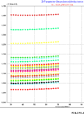
Figure 7-25 vdd_mpu Voltage/IR Drop [All Layers] Dynamic analysis of this PCB design for the MPU power domain determined the vdd_mpu decoupling capacitor loop inductance and impedance vs frequency analysis shown below. As you can see, the loop inductance values ranged from 1.0 to 1.4nH and were less than maximum 2.0nH recommended.
NOTE
Comparing loop inductances for capacitors at different distances from the processor’s input power balls shows an 18% reduction for caps placed closer. This was derived by averaging the inductances for the 3 caps with distances over 800mils (Avg LL = 1.33nH) vs the 3 caps with distances less than 600mils (Avg LL = 1.096nH).
Table 7-9 Rail - vdd_mpu
| Cap Ref Des | Model Port # | Loop Inductacne [nH] | Footprint Types | PCB Side | Distance to Ball-Field [mils] | Value [μF] | Size |
|---|---|---|---|---|---|---|---|
| C356 | 1 | 1,4 | 4vWSE | Bottom | 897 | 22 | 0603 |
| C359 | 2 | 1,26 | 4vWSE | Bottom | 855 | 2,2 | 0402 |
| C360 | 3 | 1,33 | 4vWSE | Bottom | 850 | 4,7 | 0402 |
| C365 | 4 | 1,14 | 4vWSE | Bottom | 817 | 0,1 | 0201 |
| C366 | 5 | 1,13 | 4vWSE | Bottom | 755 | 0,1 | 0201 |
| C367 | 6 | 1,07 | 4vWSE | Bottom | 758 | 1 | 0201 |
| C368 | 7 | 1,12 | 4vWSE | Bottom | 811 | 0,1 | 0201 |
| C369 | 8 | 1,06 | 4vWSE | Bottom | 690 | 0,1 | 0201 |
| C370 | 9 | 1,12 | 4vWSE | Bottom | 680 | 0,1 | 0201 |
| C384 | 10 | 1,04 | 4vWSE | Bottom | 686 | 0,1 | 0201 |
| C385 | 11 | 1,07 | 4vWSE | Top | 686 | 0,1 | 0201 |
| C387 | 12 | 1,16 | 4vWSE | Top | 755 | 0,1 | 0201 |
| C389 | 13 | 1,18 | 4vWSE | Top | 693 | 0,1 | 0201 |
| C391 | 14 | 1,14 | 4vWSE | Bottom | 693 | 0,1 | 0201 |
| C392 | 15 | 1,18 | 4vWSE | Bottom | 542 | 0,1 | 0201 |
| C396 | 16 | 1,11 | 4vWSE | Bottom | 745 | 0,1 | 0201 |
| C91 | 17 | 1,1 | 4vWSE | Bottom | 515 | 1 | 0201 |
| C92 | 18 | 1,09 | 4vWSE | Bottom | 622 | 0,22 | 0201 |
| C93 | 19 | 1,01 | 4vWSE | Bottom | 504 | 0,47 | 0201 |
| C94 | 20 | 1,13 | 4vWSE | Bottom | 604 | 0,47 | 0201 |
| C95 | 21 | 1,04 | 4vWSE | Bottom | 612 | 1 | 0201 |
| C96 | 22 | 1,08 | 4vWSE | Top | 612 | 0,22 | 0201 |
Loop Inductance range: 1,01 - 1,40 nH
 Figure 7-26 vdd_mpu Decoupling Cap Loop Inductances
 Figure 7-27 shows vdd_mpu Impedance vs Frequency characteristics.
 Figure 7-27 vdd_mpu Impedance vs Frequency