SPRS975H August 2016 – February 2020 DRA780 , DRA781 , DRA782 , DRA783 , DRA785 , DRA786 , DRA787 , DRA788
PRODUCTION DATA.
- 1Device Overview
- 2Revision History
- 3Device Comparison
-
4Terminal Configuration and Functions
- 4.1 Pin Diagram
- 4.2 Pin Attributes
- 4.3
Signal Descriptions
- 4.3.1 VIP
- 4.3.2 DSS
- 4.3.3 SD_DAC
- 4.3.4 ADC
- 4.3.5 Camera Control
- 4.3.6 CPI
- 4.3.7 CSI2
- 4.3.8 EMIF
- 4.3.9 GPMC
- 4.3.10 Timers
- 4.3.11 I2C
- 4.3.12 UART
- 4.3.13 McSPI
- 4.3.14 QSPI
- 4.3.15 McASP
- 4.3.16 DCAN and MCAN
- 4.3.17 GMAC_SW
- 4.3.18 SDIO Controller
- 4.3.19 GPIO
- 4.3.20 PWMSS
- 4.3.21 ATL
- 4.3.22 Test Interfaces
- 4.3.23 System and Miscellaneous
- 4.3.24 Power Supplies
- 4.4 Pin Multiplexing
- 4.5 Connections for Unused Pins
-
5Specifications
- 5.1 Absolute Maximum Ratings
- 5.2 ESD Ratings
- 5.3 Power-On Hours (POH)
- 5.4 Recommended Operating Conditions
- 5.5 Operating Performance Points
- 5.6 Power Consumption Summary
- 5.7
Electrical Characteristics
- Table 5-6 LVCMOS DDR DC Electrical Characteristics
- Table 5-7 Dual Voltage LVCMOS I2C DC Electrical Characteristics
- Table 5-8 IQ1833 Buffers DC Electrical Characteristics
- Table 5-9 IHHV1833 Buffers DC Electrical Characteristics
- Table 5-10 LVCMOS Analog OSC Buffers DC Electrical Characteristics
- Table 5-11 Dual Voltage LVCMOS DC Electrical Characteristics
- Table 5-12 Analog-to-Digital ADC Subsystem Electrical Specifications
- 5.8 Thermal Characteristics
- 5.9
Timing Requirements and Switching Characteristics
- 5.9.1 Timing Parameters and Information
- 5.9.2 Interface Clock Specifications
- 5.9.3 Power Supply Sequences
- 5.9.4 Clock Specifications
- 5.9.5 Recommended Clock and Control Signal Transition Behavior
- 5.9.6
Peripherals
- 5.9.6.1 Timing Test Conditions
- 5.9.6.2 VIP
- 5.9.6.3 DSS
- 5.9.6.4 EMIF
- 5.9.6.5 GPMC
- 5.9.6.6 GP Timers
- 5.9.6.7 I2C
- 5.9.6.8 UART
- 5.9.6.9 McSPI
- 5.9.6.10 QSPI
- 5.9.6.11
McASP
- Table 5-50 Timing Requirements for McASP1
- Table 5-51 Timing Requirements for McASP2
- Table 5-52 Timing Requirements for McASP3
- Table 5-53 Switching Characteristics Over Recommended Operating Conditions for McASP1
- Table 5-54 Switching Characteristics Over Recommended Operating Conditions for McASP2
- Table 5-55 Switching Characteristics Over Recommended Operating Conditions for McASP3
- 5.9.6.12 DCAN and MCAN
- 5.9.6.13
GMAC_SW
- 5.9.6.13.1 GMAC MDIO Interface Timings
- 5.9.6.13.2
GMAC RGMII Timings
- Table 5-63 Timing Requirements for rgmiin_rxc - RGMIIn Operation
- Table 5-64 Timing Requirements for GMAC RGMIIn Input Receive for 10/100/1000 Mbps
- Table 5-65 Switching Characteristics Over Recommended Operating Conditions for rgmiin_txctl - RGMIIn Operation for 10/100/1000 Mbit/s
- Table 5-66 Switching Characteristics for GMAC RGMIIn Output Transmit for 10/100/1000 Mbps
- 5.9.6.14 SDIO Controller
- 5.9.6.15 GPIO
- 5.9.6.16 ATL
- 5.9.7
Emulation and Debug Subsystem
- 5.9.7.1
JTAG Electrical Data/Timing
- Table 5-78 Timing Requirements for IEEE 1149.1 JTAG
- Table 5-79 Switching Characteristics Over Recommended Operating Conditions for IEEE 1149.1 JTAG
- Table 5-80 Timing Requirements for IEEE 1149.1 JTAG With RTCK
- Table 5-81 Switching Characteristics Over Recommended Operating Conditions for IEEE 1149.1 JTAG With RTCK
- 5.9.7.2 Trace Port Interface Unit (TPIU)
- 5.9.7.1
JTAG Electrical Data/Timing
-
6Detailed Description
- 6.1 Overview
- 6.2 Processor Subsystems
- 6.3 Accelerators and Coprocessors
- 6.4
Other Subsystems
- 6.4.1 Memory Subsystem
- 6.4.2 Interprocessor Communication
- 6.4.3 Interrupt Controller
- 6.4.4 EDMA
- 6.4.5 Peripherals
- 6.4.6 On-Chip Debug
-
7Applications, Implementation, and Layout
- 7.1 Introduction
- 7.2 Power Optimizations
- 7.3 Core Power Domains
- 7.4 Single-Ended Interfaces
- 7.5 Differential Interfaces
- 7.6 Clock Routing Guidelines
- 7.7 DDR2 Board Design and Layout Guidelines
- 7.8
DDR3 Board Design and Layout Guidelines
- 7.8.1 DDR3 General Board Layout Guidelines
- 7.8.2
DDR3 Board Design and Layout Guidelines
- 7.8.2.1 Board Designs
- 7.8.2.2 DDR3 Device Combinations
- 7.8.2.3 DDR3 Interface Schematic
- 7.8.2.4 Compatible JEDEC DDR3 Devices
- 7.8.2.5 PCB Stackup
- 7.8.2.6 Placement
- 7.8.2.7 DDR3 Keepout Region
- 7.8.2.8 Bulk Bypass Capacitors
- 7.8.2.9 High Speed Bypass Capacitors
- 7.8.2.10 Net Classes
- 7.8.2.11 DDR3 Signal Termination
- 7.8.2.12 VTT
- 7.8.2.13 CK and ADDR_CTRL Topologies and Routing Definition
- 7.8.2.14 Data Topologies and Routing Definition
- 7.8.2.15 Routing Specification
- 7.9 CVIDEO/SD-DAC Guidelines and Electrical Data/Timing
- 8Device and Documentation Support
- 9Mechanical, Packaging, and Orderable Information
Package Options
Refer to the PDF data sheet for device specific package drawings
Mechanical Data (Package|Pins)
- ABF|367
Thermal pad, mechanical data (Package|Pins)
Orderable Information
5.9.6.5.2 GPMC/NOR Flash Interface Asynchronous Timing
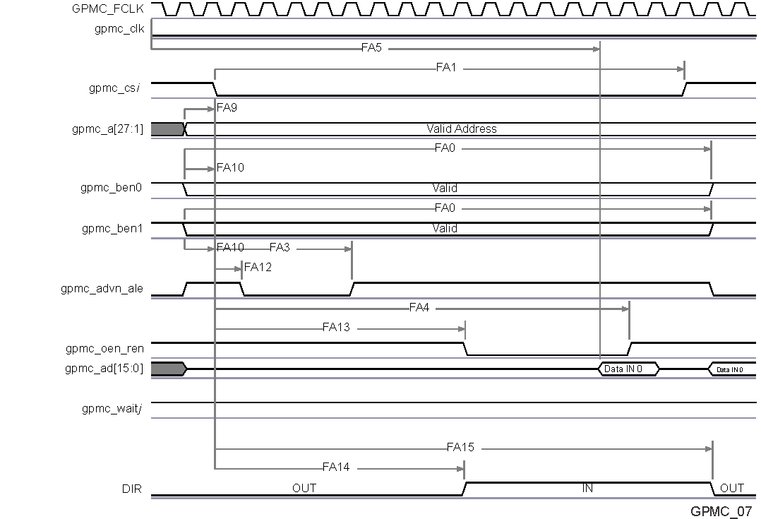
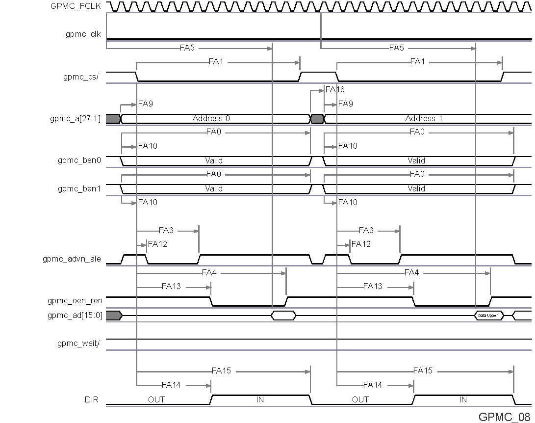
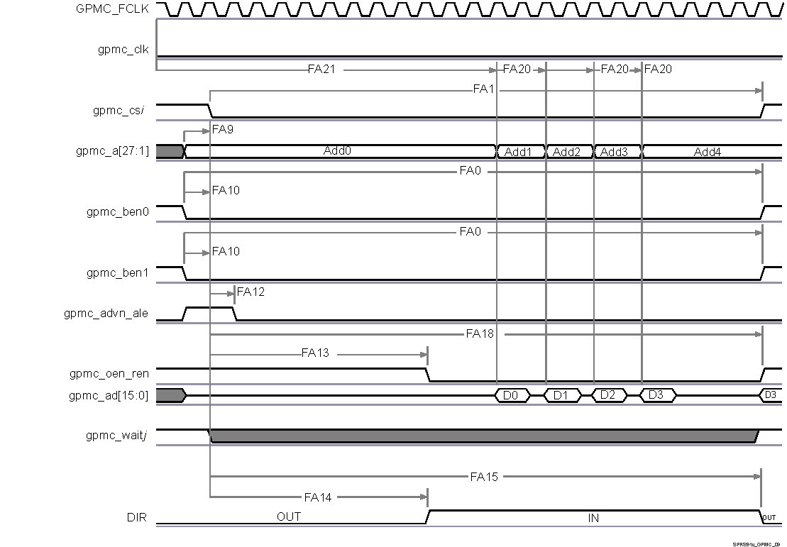
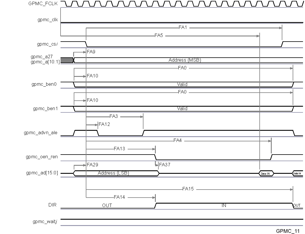
Table 5-35 and Table 5-36 assume testing over the recommended operating conditions and electrical characteristic conditions below (see Figure 5-28, Figure 5-29, Figure 5-30, Figure 5-31, Figure 5-32 and Figure 5-33).
Table 5-35 GPMC/NOR Flash Interface Timing Requirements - Asynchronous Mode
| NO. | PARAMETER | DESCRIPTION | MIN | MAX | UNIT | |
|---|---|---|---|---|---|---|
| FA5 | tacc(DAT) | Data Maximum Access Time (GPMC_FCLK cycles) | H (1) | cycles | ||
| FA20 | tacc1-pgmode(DAT) | Page Mode Successive Data Maximum Access Time (GPMC_FCLK cycles) | P (2) | cycles | ||
| FA21 | tacc2-pgmode(DAT) | Page Mode First Data Maximum Access Time (GPMC_FCLK cycles) | H (1) | cycles | ||
| - | tsu(DV-OEH) | Setup time, read gpmc_ad[15:0] valid before gpmc_oen_ren high | 1.9 | ns | ||
| - | - | th(OEH-DV) | Hold time, read gpmc_ad[15:0] valid after gpmc_oen_ren high | 1 | ns |
- H = Access Time × (TimeParaGranularity + 1)
- P = PageBurstAccessTime × (TimeParaGranularity + 1)
Table 5-36 GPMC/NOR Flash Interface Switching Characteristics - Asynchronous Mode
| NO. | PARAMETER | DESCRIPTION | MIN | MAX | UNIT | |
|---|---|---|---|---|---|---|
| - | tr(DO) | Rising time, gpmc_ad[15:0] output data | 0.447 | 4.067 | ns | |
| - | - | tf(DO) | Fallling time, gpmc_ad[15:0] output data | 0.43 | 4.463 | ns |
| FA0 | tw(nBEV) | Pulse duration, gpmc_ben[1:0] valid time | N | ns | ||
| FA1 | tw(nCSV) | Pulse duration, gpmc_cs[7:0] low | A | ns | ||
| FA3 | td(nCSV-nADVIV) | Delay time, gpmc_cs[7:0] valid to gpmc_advn_ale invalid | B - 0.2 | B + 2.0 | ns | |
| FA4 | td(nCSV-nOEIV) | Delay time, gpmc_cs[7:0] valid to gpmc_oen_ren invalid (Single read) | C - 0.2 | C + 2.0 | ns | |
| FA9 | td(AV-nCSV) | Delay time, address bus valid to gpmc_cs[7:0] valid | J - 0.2 | J + 2.0 | ns | |
| FA10 | td(nBEV-nCSV) | Delay time, gpmc_ben[1:0] valid to gpmc_cs[7:0] valid | J - 0.2 | J + 2.0 | ns | |
| FA12 | td(nCSV-nADVV) | Delay time, gpmc_cs[7:0] valid to gpmc_advn_ale valid | K - 0.2 | K + 2.0 | ns | |
| FA13 | td(nCSV-nOEV) | Delay time, gpmc_cs[7:0] valid to gpmc_oen_ren valid | L - 0.2 | L + 2.0 | ns | |
| FA16 | tw(AIV) | Pulse duration, address invalid between 2 successive R/W accesses | G | ns | ||
| FA18 | td(nCSV-nOEIV) | Delay time, gpmc_cs[7:0] valid to gpmc_oen_ren invalid (Burst read) | I - 0.2 | I + 2.0 | ns | |
| FA20 | tw(AV) | Pulse duration, address valid : 2nd, 3rd and 4th accesses | D | ns | ||
| FA25 | td(nCSV-nWEV) | Delay time, gpmc_cs[7:0] valid to gpmc_wen valid | E - 2 | E + 2.0 | ns | |
| FA27 | td(nCSV-nWEIV) | Delay time, gpmc_cs[7:0] valid to gpmc_wen invalid | F - 0.2 | F + 2.0 | ns | |
| FA28 | td(nWEV-DV) | Delay time, gpmc_ wen valid to data bus valid | 2 | ns | ||
| FA29 | td(DV-nCSV) | Delay time, data bus valid to gpmc_cs[7:0] valid | J - 0.2 | J + 2.0 | ns | |
| FA37 | td(nOEV-AIV) | Delay time, gpmc_oen_ren valid to gpmc_ad[15:0] multiplexed address bus phase end | 2 | ns |
- For single read: N = RdCycleTime × (TimeParaGranularity + 1) × GPMC_FCLK
For single write: N = WrCycleTime × (TimeParaGranularity + 1) × GPMC_FCLK
For burst read: N = (RdCycleTime + (n – 1) × PageBurstAccessTime) × (TimeParaGranularity + 1) × GPMC_FCLK
For burst write: N = (WrCycleTime + (n – 1) × PageBurstAccessTime) × (TimeParaGranularity + 1) × GPMC_FCLK - For single read: A = (CSRdOffTime - CSOnTime) × (TimeParaGranularity + 1) × GPMC_FCLK
For single write: A = (CSWrOffTime – CSOnTime) × (TimeParaGranularity + 1) × GPMC_FCLK
For burst read: A = (CSRdOffTime - CSOnTime + (n - 1) × PageBurstAccessTime) × (TimeParaGranularity + 1) × GPMC_FCLK period
For burst write: A = (CSWrOffTime - CSOnTime + (n - 1) × PageBurstAccessTime) × (TimeParaGranularity + 1) × GPMC_FCLK period with n the page burst access number. - For reading: B = ((ADVRdOffTime – CSOnTime) × (TimeParaGranularity + 1) + 0.5 × (ADVExtraDelay – CSExtraDelay)) × GPMC_FCLK
For writing: B = ((ADVWrOffTime – CSOnTime) × (TimeParaGranularity + 1) + 0.5 × (ADVExtraDelay – CSExtraDelay)) × GPMC_FCLK - C = ((OEOffTime – CSOnTime) × (TimeParaGranularity + 1) + 0.5 × (OEExtraDelay – CSExtraDelay)) × GPMC_FCLKFor single read: C = RdCycleTime × (TimeParaGranularity + 1) × GPMC_FCLK
- J = (CSOnTime × (TimeParaGranularity + 1) + 0.5 × CSExtraDelay) × GPMC_FCLK
- K = ((ADVOnTime – CSOnTime) × (TimeParaGranularity + 1) + 0.5 × (ADVExtraDelay – CSExtraDelay)) × GPMC_FCLK
- L = ((OEOnTime – CSOnTime) × (TimeParaGranularity + 1) + 0.5 × (OEExtraDelay – CSExtraDelay)) × GPMC_FCLK
- G = Cycle2CycleDelay × GPMC_FCLK × (TimeParaGranularity + 1)
- I = ((OEOffTime + (n – 1) × PageBurstAccessTime – CSOnTime) × (TimeParaGranularity + 1) + 0.5 × (OEExtraDelay – CSExtraDelay)) × GPMC_FCLK
- D = PageBurstAccessTime × (TimeParaGranularity + 1) × GPMC_FCLK
- E = ((WEOnTime – CSOnTime) × (TimeParaGranularity + 1) + 0.5 × (WEExtraDelay – CSExtraDelay)) × GPMC_FCLK
- F = ((WEOffTime – CSOnTime) × (TimeParaGranularity + 1) + 0.5 × (WEExtraDelay – CSExtraDelay)) × GPMC_FCLK
- In gpmc_csi, i = 0 to 7. In gpmc_waitj, j = 0 to 1.
- FA5 parameter illustrates amount of time required to internally sample input data. It is expressed in number of GPMC functional clock cycles. From start of read cycle and after FA5 functional clock cycles, input Data will be internally sampled by active functional clock edge. FA5 value must be stored inside AccessTime register bits field.
- GPMC_FCLK is an internal clock (GPMC functional clock) not provided externally.
- The "DIR" (direction control) output signal is NOT pinned out on any of the device pads. It is an internal signal only representing a signal direction on the GPMC data bus.
- In “gpmc_csi”, i = 0 to 7. In “gpmc_waitj”, j = 0 to 1.
- FA5 parameter illustrates amount of time required to internally sample input Data. It is expressed in number of GPMC functional clock cycles. From start of read cycle and after FA5 functional clock cycles, input Data will be internally sampled by active functional clock edge. FA5 value should be stored inside AccessTime register bits field
- GPMC_FCLK is an internal clock (GPMC functional clock) not provided externally
- The "DIR" (direction control) output signal is NOT pinned out on any of the device pads. It is an internal signal only representing a signal direction on the GPMC data bus.
- In “gpmc_csi”, i = 0 to 7. In “gpmc_waitj”, j = 0 to 1
- FA21 parameter illustrates amount of time required to internally sample first input Page Data. It is expressed in number of GPMC functional clock cycles. From start of read cycle and after FA21 functional clock cycles, First input Page Data will be internally sampled by active functional clock edge. FA21 calculation is detailled in a separated application note (ref …) and should be stored inside AccessTime register bits field.
- FA20 parameter illustrates amount of time required to internally sample successive input Page Data. It is expressed in number of GPMC functional clock cycles. After each access to input Page Data, next input Page Data will be internally sampled by active functional clock edge after FA20 functional clock cycles. FA20 is also the duration of address phases for successive input Page Data (excluding first input Page Data). FA20 value should be stored in PageBurstAccessTime register bits field.
- GPMC_FCLK is an internal clock (GPMC functional clock) not provided externally
- The "DIR" (direction control) output signal is NOT pinned out on any of the device pads. It is an internal signal only representing a signal direction on the GPMC data bus.
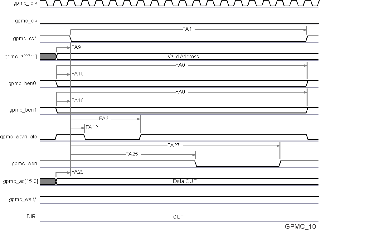 Figure 5-31 GPMC / NOR Flash - Asynchronous Write - Single Word Timing(1)
 - In “gpmc_csi”, i = 0 to 7. In “gpmc_waitj”, j = 0 to 1.
- The "DIR" (direction control) output signal is NOT pinned out on any of the device pads. It is an internal signal only representing a signal direction on the GPMC data bus.
- In “gpmc_csi”, i = 0 to 7. In “gpmc_waitj”, j = 0 to 1
- FA5 parameter illustrates amount of time required to internally sample input Data. It is expressed in number of GPMC functional clock cycles. From start of read cycle and after FA5 functional clock cycles, input Data will be internally sampled by active functional clock edge. FA5 value should be stored inside AccessTime register bits field.
- GPMC_FCLK is an internal clock (GPMC functional clock) not provided externally
- The "DIR" (direction control) output signal is NOT pinned out on any of the device pads. It is an internal signal only representing a signal direction on the GPMC data bus.
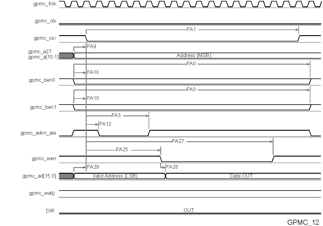 Figure 5-33 GPMC / Multiplexed NOR Flash - Asynchronous Write - Single Word Timing(1)
 - In “gpmc_csi”, i = 0 to 7. In “gpmc_waitj”, j = 0 to 1.
- The "DIR" (direction control) output signal is NOT pinned out on any of the device pads. It is an internal signal only representing a signal direction on the GPMC data bus.
